- 您现在的位置:买卖IC网 > PDF目录3766 > MAX7314AEG+T (Maxim Integrated Products)IC I/O EXPANDER I2C 16B 24QSOP PDF资料下载
参数资料
| 型号: | MAX7314AEG+T |
| 厂商: | Maxim Integrated Products |
| 文件页数: | 23/25页 |
| 文件大小: | 0K |
| 描述: | IC I/O EXPANDER I2C 16B 24QSOP |
| 产品培训模块: | Lead (SnPb) Finish for COTS Obsolescence Mitigation Program |
| 标准包装: | 2,500 |
| 接口: | I²C |
| 输入/输出数: | 18 |
| 中断输出: | 是 |
| 频率 - 时钟: | 400kHz |
| 电源电压: | 2 V ~ 3.6 V |
| 工作温度: | -40°C ~ 125°C |
| 安装类型: | 表面贴装 |
| 封装/外壳: | 24-SSOP(0.154",3.90mm 宽) |
| 供应商设备封装: | 24-QSOP |
| 包装: | 带卷 (TR) |
Port Inputs and Transition Detection
Input ports registers reflect the incoming logic levels of
the port pins, regardless of whether the pin is defined
as an input or an output. Reading an input ports regis-
ter latches the current-input logic level of the affected
eight ports. Transition detection allows all ports config-
ured as inputs to be monitored for changes in their
logic status. The action of reading an input ports regis-
ter samples the corresponding 8 port bits’ input condi-
tion. This sample is continuously compared with the
actual input conditions. A detected change in input
condition causes the INT/O16 interrupt output to go
low, if configured as an interrupt output. The interrupt is
cleared either automatically if the changed input
returns to its original state, or when the appropriate
input ports register is read.
The INT/O16 pin can be configured as either an inter-
rupt output or as a 17th output port with the same static
or blink controls as the other 16 ports (Table 4).
Port Output Control and LED Blinking
The two blink phase 0 registers set the output logic lev-
els of the 16 ports P0–P15 (Table 8). These registers
control the port outputs if the blink function is disabled.
A duplicate pair of registers, the blink phase 1 registers,
are also used if the blink function is enabled (Table 9).
In blink mode, the port outputs can be flipped between
using the blink phase 0 registers and the blink phase 1
registers using hardware control (the BLINK input)
and/or software control (the blink flip flag in the configu-
ration register) (Table 4). The logic level of the BLINK
input can be read back through the blink status bit in
the configuration register (Table 4). The BLINK input,
therefore, can be used as a general-purpose logic input
(GPI port) if the blink function is not required.
PWM Intensity Control
The MAX7314 includes an internal oscillator, nominally
32kHz, to generate PWM timing for LED intensity control.
PWM intensity control can be enabled on an output-by-
output basis, allowing the MAX7314 to provide any mix
of PWM LED drives and glitch-free logic outputs (Table
10). PWM can be disabled entirely, in which case all out-
put ports are static and the MAX7314 operating current
is lowest because the internal oscillator is turned off.
PWM intensity control uses a 4-bit master control and 4
bits of individual control per output (Tables 13, 14). The
4-bit master control provides 16 levels of overall intensi-
ty control, which applies to all PWM-enabled output
ports. The master control sets the maximum pulse
width from 1/15 to 15/15 of the PWM time period. The
individual settings comprise a 4-bit number, further
reducing the duty cycle to be from 1/16 to 15/16 of the
time window set by the master control.
For applications requiring the same PWM setting for all
output ports, a single global PWM control can be used
instead of all the individual controls to simplify the con-
trol software and provide 240 steps of intensity control
(Tables 10 and 13).
Standby Mode
When the serial interface is idle and the PWM intensity
control is unused, the MAX7314 automatically enters
standby mode. If the PWM intensity control is used, the
operating current is slightly higher because the internal
PWM oscillator is running. When the serial interface is
active, the operating current also increases because
the MAX7314, like all I2C slaves, has to monitor every
transmission.
MAX7314
18-Port GPIO with LED Intensity Control,
Interrupt, and Hot-Insertion Protection
_______________________________________________________________________________________
7
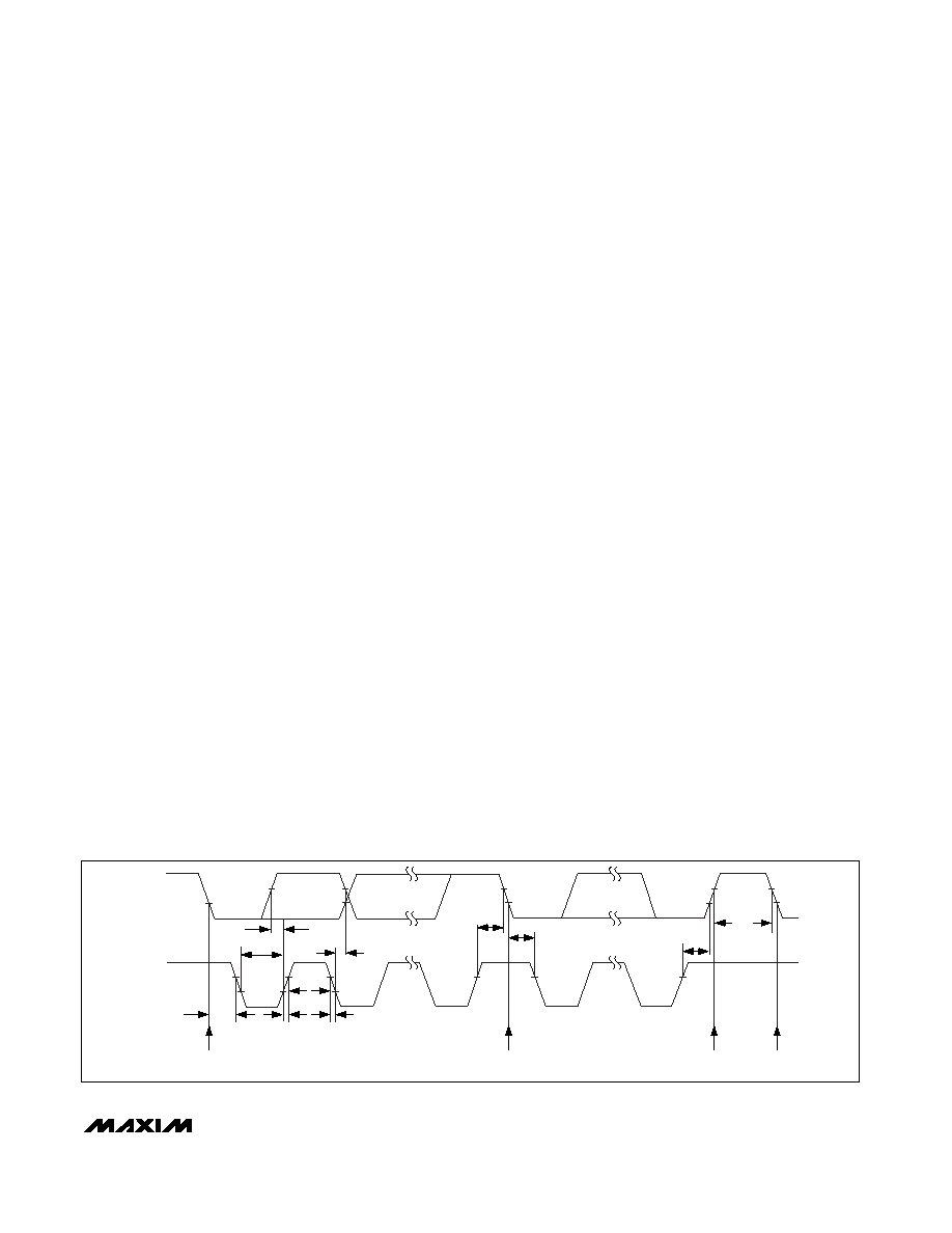
Figure 2. 2-Wire Serial Interface Timing Details
SCL
SDA
tR
tF
tBUF
START
CONDITION
STOP
CONDITION
REPEATED START CONDITION
START CONDITION
tSU,STO
tHD,STA
tSU,STA
tHD,DAT
tSU,DAT
tLOW
tHIGH
tHD,STA
相关PDF资料 |
PDF描述 |
|---|---|
| ST16C550IQ48-F | IC UART FIFO 16B SGL 48TQFP |
| MAX7318AWG+T | IC PORT EXPANDER 16BIT 24SOIC |
| XR20M1170IL24-F | IC UART FIFO I2C/SPI 64B 24QFN |
| MAX7318AAG+T | IC I/O EXPANDER I2C 16B 24SSOP |
| MAX7318AUG+T | IC I/O EXPANDER I2C 16B 24TSSOP |
相关代理商/技术参数 |
参数描述 |
|---|---|
| MAX7314ATG | 功能描述:外围驱动器与原件 - PCI RoHS:否 制造商:PLX Technology 工作电源电压: 最大工作温度: 安装风格:SMD/SMT 封装 / 箱体:FCBGA-1156 封装:Tray |
| MAX7314ATG+ | 功能描述:外围驱动器与原件 - PCI 18-Port GPIO RoHS:否 制造商:PLX Technology 工作电源电压: 最大工作温度: 安装风格:SMD/SMT 封装 / 箱体:FCBGA-1156 封装:Tray |
| MAX7314ATG+T | 功能描述:接口-I/O扩展器 18-Port GPIO RoHS:否 制造商:NXP Semiconductors 逻辑系列: 输入/输出端数量: 最大工作频率:100 kHz 工作电源电压:1.65 V to 5.5 V 工作温度范围:- 40 C to + 85 C 安装风格:SMD/SMT 封装 / 箱体:HVQFN-16 封装:Reel |
| MAX7314ATG-T | 功能描述:外围驱动器与原件 - PCI RoHS:否 制造商:PLX Technology 工作电源电压: 最大工作温度: 安装风格:SMD/SMT 封装 / 箱体:FCBGA-1156 封装:Tray |
| MAX7314EVKIT+ | 功能描述:外围驱动器与原件 - PCI Evaluation Kit for the MAX7314 RoHS:否 制造商:PLX Technology 工作电源电压: 最大工作温度: 安装风格:SMD/SMT 封装 / 箱体:FCBGA-1156 封装:Tray |
发布紧急采购,3分钟左右您将得到回复。