- 您现在的位置:买卖IC网 > PDF目录3766 > MAX7314AEG+T (Maxim Integrated Products)IC I/O EXPANDER I2C 16B 24QSOP PDF资料下载
参数资料
| 型号: | MAX7314AEG+T |
| 厂商: | Maxim Integrated Products |
| 文件页数: | 25/25页 |
| 文件大小: | 0K |
| 描述: | IC I/O EXPANDER I2C 16B 24QSOP |
| 产品培训模块: | Lead (SnPb) Finish for COTS Obsolescence Mitigation Program |
| 标准包装: | 2,500 |
| 接口: | I²C |
| 输入/输出数: | 18 |
| 中断输出: | 是 |
| 频率 - 时钟: | 400kHz |
| 电源电压: | 2 V ~ 3.6 V |
| 工作温度: | -40°C ~ 125°C |
| 安装类型: | 表面贴装 |
| 封装/外壳: | 24-SSOP(0.154",3.90mm 宽) |
| 供应商设备封装: | 24-QSOP |
| 包装: | 带卷 (TR) |
The second (A5), third (A4), fourth (A3), sixth (A1), and
last (A0) bits of the MAX7314 slave address are always
1, 0, 0, 0, and 0. Slave address bits A6 and A2 are
selected by the address input AD0. AD0 can be con-
nected to GND, V+, SDA, or SCL. The MAX7314 has four
possible slave addresses (Table 1), and therefore a
maximum of four MAX7314 devices can be controlled
independently from the same interface.
Message Format for Writing the MAX7314
A write to the MAX7314 comprises the transmission of
the MAX7314’s slave address with the R/W bit set to
zero, followed by at least 1 byte of information. The first
byte of information is the command byte. The com-
mand byte determines which register of the MAX7314
is to be written to by the next byte, if received (Table 2).
If a STOP condition is detected after the command byte
is received, then the MAX7314 takes no further action
beyond storing the command byte.
Any bytes received after the command byte are data
bytes. The first data byte goes into the internal register
of the MAX7314 selected by the command byte (Figure
8). If multiple data bytes are transmitted before a STOP
condition is detected, these bytes are generally stored
in subsequent MAX7314 internal registers because the
command byte address autoincrements (Table 2). A
diagram of a write to the output ports registers (blink
phase 0 registers or blink phase 1 registers) is given in
Figure 10.
MAX7314
18-Port GPIO with LED Intensity Control,
Interrupt, and Hot-Insertion Protection
_______________________________________________________________________________________
9
Table 1. MAX7314 Address Map
DEVICE ADDRESS
PIN AD0
A6
A5
A4
A3
A2
A1
A0
SCL
1
100
000
SDA
1
100
GND
0
100
000
V+
0
100
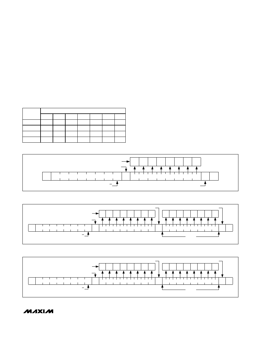
Figure 8. Command and Single Data Byte Received
SA
A
P
0
SLAVE ADDRESS
COMMAND BYTE
DATA BYTE
1
BYTE
AUTOINCREMENT MEMORY ADDRESS
D15 D14 D13 D12 D11 D10
D9
D8
D1
D0
D3
D2
D5
D4
D7
D6
ACKNOWLEDGE FROM MAX7314
HOW COMMAND BYTE AND DATA BYTE MAP INTO
MAX7314's REGISTERS
R/W
Figure 9. n Data Bytes Received
SA
A
P
0
SLAVE ADDRESS
COMMAND BYTE
DATA BYTE
N
BYTES
AUTOINCREMENT MEMORY ADDRESS
D15 D14 D13 D12 D11 D10
D9
D8
D1
D0
D3
D2
D5
D4
D7
D6
ACKNOWLEDGE FROM MAX7314
HOW COMMAND BYTE AND DATA BYTE MAP INTO
MAX7314's REGISTERS
R/W
Figure 7. Command Byte Received
SA
A
P
0
SLAVE ADDRESS
COMMAND BYTE
ACKNOWLEDGE FROM MAX7314
D15
D14
D13
D12
D11
D10
D9
D8
COMMAND BYTE IS STORED ON RECEIPT OF
STOP CONDITION
ACKNOWLEDGE FROM MAX7314
R/W
相关PDF资料 |
PDF描述 |
|---|---|
| ST16C550IQ48-F | IC UART FIFO 16B SGL 48TQFP |
| MAX7318AWG+T | IC PORT EXPANDER 16BIT 24SOIC |
| XR20M1170IL24-F | IC UART FIFO I2C/SPI 64B 24QFN |
| MAX7318AAG+T | IC I/O EXPANDER I2C 16B 24SSOP |
| MAX7318AUG+T | IC I/O EXPANDER I2C 16B 24TSSOP |
相关代理商/技术参数 |
参数描述 |
|---|---|
| MAX7314ATG | 功能描述:外围驱动器与原件 - PCI RoHS:否 制造商:PLX Technology 工作电源电压: 最大工作温度: 安装风格:SMD/SMT 封装 / 箱体:FCBGA-1156 封装:Tray |
| MAX7314ATG+ | 功能描述:外围驱动器与原件 - PCI 18-Port GPIO RoHS:否 制造商:PLX Technology 工作电源电压: 最大工作温度: 安装风格:SMD/SMT 封装 / 箱体:FCBGA-1156 封装:Tray |
| MAX7314ATG+T | 功能描述:接口-I/O扩展器 18-Port GPIO RoHS:否 制造商:NXP Semiconductors 逻辑系列: 输入/输出端数量: 最大工作频率:100 kHz 工作电源电压:1.65 V to 5.5 V 工作温度范围:- 40 C to + 85 C 安装风格:SMD/SMT 封装 / 箱体:HVQFN-16 封装:Reel |
| MAX7314ATG-T | 功能描述:外围驱动器与原件 - PCI RoHS:否 制造商:PLX Technology 工作电源电压: 最大工作温度: 安装风格:SMD/SMT 封装 / 箱体:FCBGA-1156 封装:Tray |
| MAX7314EVKIT+ | 功能描述:外围驱动器与原件 - PCI Evaluation Kit for the MAX7314 RoHS:否 制造商:PLX Technology 工作电源电压: 最大工作温度: 安装风格:SMD/SMT 封装 / 箱体:FCBGA-1156 封装:Tray |
发布紧急采购,3分钟左右您将得到回复。