- 您现在的位置:买卖IC网 > PDF目录10618 > MAX7456EUI+ (Maxim Integrated Products)IC ON-SCREEN DISPLAY 28-TSSOP PDF资料下载
参数资料
| 型号: | MAX7456EUI+ |
| 厂商: | Maxim Integrated Products |
| 文件页数: | 44/44页 |
| 文件大小: | 0K |
| 描述: | IC ON-SCREEN DISPLAY 28-TSSOP |
| 产品培训模块: | Lead (SnPb) Finish for COTS Obsolescence Mitigation Program |
| 标准包装: | 50 |
| 类型: | OSD(屏幕显示)视频发生器 |
| 应用: | 安全系统,视频路由 |
| 安装类型: | 表面贴装 |
| 封装/外壳: | 28-SOIC(0.173",4.40mm 宽)裸露焊盘 |
| 供应商设备封装: | 28-TSSOP 裸露焊盘 |
| 包装: | 管件 |
| 产品目录页面: | 1424 (CN2011-ZH PDF) |
第1页第2页第3页第4页第5页第6页第7页第8页第9页第10页第11页第12页第13页第14页第15页第16页第17页第18页第19页第20页第21页第22页第23页第24页第25页第26页第27页第28页第29页第30页第31页第32页第33页第34页第35页第36页第37页第38页第39页第40页第41页第42页第43页当前第44页
Single-Channel Monochrome On-Screen
Display with Integrated EEPROM
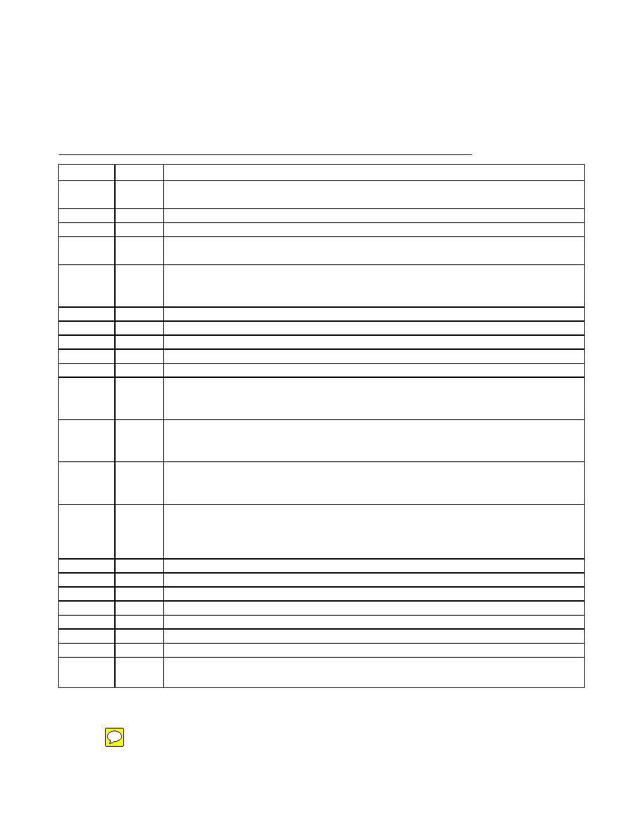
Pin Description
PIN
NAME
FUNCTION
1, 2, 13–16,
27, 28
N.C.
No Connection. Not internally connected.
3
DVDD
Digital Power-Supply Input. Bypass to DGND with a 0.1F capacitor.
4
DGND
Digital Ground
5
CLKIN
Crystal Connection 1. Connect a parallel resonant, fundamental mode crystal between CLKIN and XFB
for use as a crystal oscillator, or drive CLKIN directly with a 27MHz system reference clock.
6
XFB
Crystal Connection 2. Connect a parallel resonant, fundamental mode crystal between CLKIN and XFB
for use as a crystal oscillator, or leave XFB unconnected when driving CLKIN with a 27MHz system
reference clock.
7
CLKOUT
Clock Output. 27MHz logic-level output system clock.
8
CS
Active-Low Chip-Select Input. SDOUT goes high impedance when CS is high.
9
SDIN
Serial Data Input. Data is clocked in at rising edge of SCLK.
10
SCLK
Serial Clock Input. Clocks data into SDIN and out of SDOUT. Duty cycle must be between 40% and 60%.
11
SDOUT
Serial Data Output. Data is clocked out at the falling edge of SCLK. High impedance when CS is high.
12
LOS
Loss-of-Sync Output (Open-Drain). LOS goes high when the VIN sync pulse is lost for 32 consecutive
lines. LOS goes low when 32 consecutive valid sync pulses are received. Connect to a 1k
Ω pullup
resistor to DVDD or another positive supply voltage suitable for the receiving device.
17
VSYNC
Vertical Sync Output (Open-Drain). VSYNC goes low following the video input’s vertical sync interval.
VSYNC is either recovered from VIN or internally generated when in internal sync mode. Connect to a
1k
Ω pullup resistor to DVDD or another positive supply voltage suitable for the receiving device.
18
HSYNC
Horizontal Sync Output (Open-Drain). HSYNC goes low following the video input’s horizontal sync
interval. HSYNC is either recovered from VIN or internally generated when in internal sync mode. Connect
to a 1k
Ω pullup resistor to DVDD or another positive supply voltage suitable for the receiving device.
19
RESET
System Reset Input. The minimum RESET pulse width is 50ms. All SPI registers are reset to their default
values after 100s following the rising edge of RESET. These registers are not accessible for reading or
writing during that time. The display memory is reset to its default value of 00H in all locations after 20s
following the rising edge of RESET.
20
AGND
Analog Ground
21
AVDD
Analog Power-Supply Input. Bypass to AGND with a 0.1F capacitor.
22
VIN
PAL or NTSC CVBS Video Input
23
PGND
Driver Ground. Connect to AGND at a single point.
24
PVDD
Driver Power-Supply Input. Bypass to PGND with a 0.1F capacitor.
25
SAG
Sag Correction Input. Connect to VOUT if not used. See Figure 1b.
26
VOUT
Video Output
—EP
Exposed Pad. Internally connected to AGND. Connect EP to the AGND plane for improved heat
dissipation. Do not use EP as the only ground connection.
MAX7456
Maxim Integrated
9
相关PDF资料 |
PDF描述 |
|---|---|
| MAX242EPN+ | IC TXRX RS232 5V 18-DIP |
| MAX3815CCM+D | IC EQUALIZER VIDEO 48-TQFP |
| MAX9135GHJ+ | IC SW LVDS CROSSBAR 32TQFP-EP |
| MAX242EWN+ | IC TXRX RS232 5V 18-SOIC |
| MAX9134GHJ+ | IC SW LVDS CROSSBAR 32TQFP-EP |
相关代理商/技术参数 |
参数描述 |
|---|---|
| MAX7456EUI/GH9 | 制造商:Maxim Integrated Products 功能描述:SINGLE-CHANNEL MONOCHROME ON-SCREEN DISPLAY - Rail/Tube |
| MAX7456EUI+ | 功能描述:视频 IC Monochrome On Scrn Display Generator RoHS:否 制造商:Fairchild Semiconductor 工作电源电压:5 V 电源电流:80 mA 最大工作温度:+ 85 C 封装 / 箱体:TSSOP-28 封装:Reel |
| MAX7456EUI+T | 功能描述:视频 IC Monochrome On Scrn Display Generator RoHS:否 制造商:Fairchild Semiconductor 工作电源电压:5 V 电源电流:80 mA 最大工作温度:+ 85 C 封装 / 箱体:TSSOP-28 封装:Reel |
| MAX7456EUI+W | 制造商:Maxim Integrated Products 功能描述:- Rail/Tube |
| MAX7456EVKIT | 功能描述:显示开发工具 RoHS:否 制造商:4D Systems 产品:4Display Shields 工具用于评估:?OLED-160-G1, ?OLED-160-G2 接口类型:Serial 工作电源电压:5 V |
发布紧急采购,3分钟左右您将得到回复。