- 您现在的位置:买卖IC网 > Datasheet目录341 > MAX8513EVKIT (Maxim Integrated Products)EVAL KIT FOR MAX8513 Datasheet资料下载
参数资料
| 型号: | MAX8513EVKIT |
| 厂商: | Maxim Integrated Products |
| 文件页数: | 13/35页 |
| 文件大小: | 0K |
| 描述: | EVAL KIT FOR MAX8513 |
| 产品培训模块: | Lead (SnPb) Finish for COTS Obsolescence Mitigation Program |
| 标准包装: | 1 |
| 主要目的: | DC/DC,LDO 步降 |
| 输出及类型: | 3,非隔离 |
| 输出电压: | 3.3V,2.5V,12V |
| 电流 - 输出: | 2A,1.5A,100mA |
| 输入电压: | 9 ~ 16 V |
| 稳压器拓扑结构: | 降压 |
| 频率 - 开关: | 1.4MHz |
| 板类型: | 完全填充 |
| 已供物品: | 板 |
| 已用 IC / 零件: | MAX8513 |
第1页第2页第3页第4页第5页第6页第7页第8页第9页第10页第11页第12页当前第13页第14页第15页第16页第17页第18页第19页第20页第21页第22页第23页第24页第25页第26页第27页第28页第29页第30页第31页第32页第33页第34页第35页
�� �
�
�Wide-Input,� High-Frequency,� Triple-Output� Supplies�
�with� Voltage� Monitor� and� Power-On� Reset�
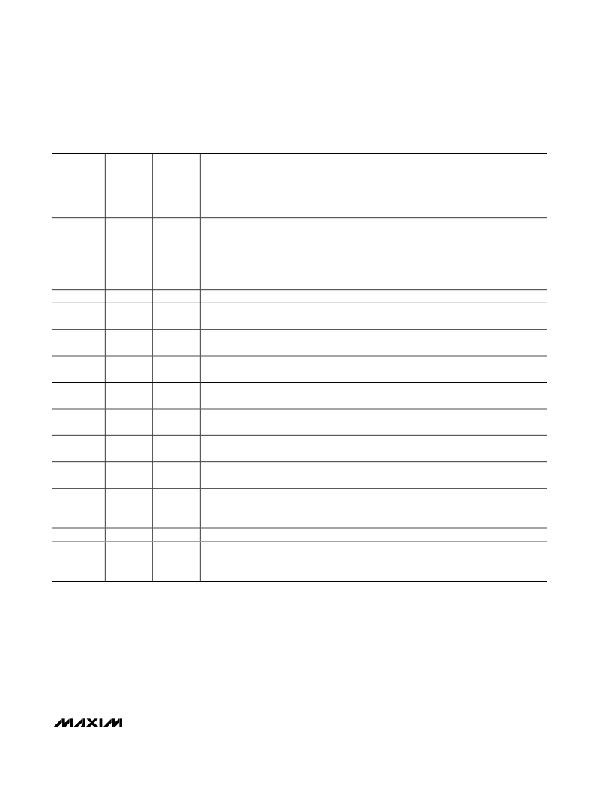
�Pin� Description� (continued)�
�PIN�
�NAME�
�MAX8513�
�MAX8514�
�FUNCTION�
�Connect� to� VL� for� output� tracking.� Connect� to� GND� for� output� staggered� sequence.�
�SEQ�
�18�
�18�
�Staggered� sequence� ramps� up� V� OUT2� and� V� OUT3� softly� to� avoid� glitches� on� the� previous�
�voltage� due� to� charging� of� the� LDO’s� output� capacitors.�
�Shutdown� Control� and� Synchronization� Input.� There� are� three� operating� modes:�
�?� When� SYNC/EN� is� low,� the� controller� is� off� but� the� VL� regulator� is� still� running.�
�SYNC/EN�
�19�
�19�
�?� When� SYNC/EN� is� high,� the� controller� is� enabled� with� the� switching� frequency� set� by�
�R� FREQ� .�
�?� When� SYNC/EN� is� driven� by� an� external� clock,� the� controller� is� enabled� and� switches� at�
�the� external� clock� frequency.�
�N.C.�
�SUP3N�
�DRV3P�
�DRV3N�
�IN�
�POR�
�FB3P�
�FB3N�
�ILIM�
�CSP�
�CSN�
�20�
�—�
�21�
�—�
�22�
�23�
�24�
�—�
�25�
�26�
�27�
�—�
�20�
�—�
�21�
�22�
�23�
�—�
�24�
�25�
�26�
�27�
�No� Connection.� Not� internally� connected.� Connect� to� GND� or� leave� floating.�
�OUT3N� Base-Drive� Supply.� Connect� SUP3N� to� any� positive� voltage� between� 1.5V� and� 5.5V�
�to� provide� power� for� the� negative� linear-regulator� transistor� driver.�
�OUT3P� Base� Drive.� Connect� DRV3P� to� the� base� of� an� external� PNP� pass� transistor� to� form� a�
�positive� linear� voltage� regulator.�
�OUT3N� Base� Drive.� Connect� DRV3N� to� the� base� of� an� external� NPN� pass� transistor� to� form�
�a� negative� linear� voltage� regulator.�
�Main� Voltage� Input� (4.5V� to� 28V).� Bypass� IN� to� GND,� close� to� the� IC,� with� a� minimum� 1μF�
�ceramic� capacitor� (C2).� IN� powers� the� linear� regulator� whose� output� is� VL.�
�Power-On� Reset.� Open-drain� output� that� goes� high� after� all� outputs� reach� the� regulation�
�limit� and� a� 315ms� delay� time� has� elapsed.�
�OUT3P� Feedback� Input.� FB3P� is� referenced� to� 0.8V� and� connects� to� a� resistive-divider�
�(R13,� R14)� to� control� a� positive� linear� voltage� regulator.�
�OUT3N� Feedback� Input.� Connect� a� resistive-divider� (R13,� R14)� from� OUT1� to� FB3N� to�
�OUT3N� to� regulate� FB3N� to� 0V.�
�ILIM� Set� Input.� Connect� a� resistive-divider� (R17,� R18)� from� OUT1� to� ILIM� to� GND.� See� the�
�Current� Limit� section.�
�Positive� Current-Sense� Input.� Used� to� detect� OUT1� current� limit.�
�Negative� Current-Sense� Input.� Used� to� detect� OUT1� current� limit.�
�Analog� Soft-Start� Control� Input.� This� pin� goes� into� the� positive� input� of� the� VOUT1’s� error�
�SS�
�28�
�28�
�amplifier.� When� the� MAX8513/MAX8514� are� turned� on,� SS� is� at� GND� and� charges� up� to� 1.25V�
�with� a� constant� 25μA.� Connect� a� capacitor� (C13)� from� SS� to� GND� for� the� desired� soft-start� time.�
�______________________________________________________________________________________�
�13�
�相关PDF资料 |
PDF描述 |
|---|---|
| MAX8552EUB+ | IC DRIVER MOSFET HS 10-UMAX |
| MAX8595XETA+T | IC LED DRIVR WHITE BCKLGT 8-TDFN |
| MAX8607ETD+T | IC LED DRIVR PHOTO FLASH 14-TDFN |
| MAX8608YETD+T | IC LED DRVR WT/OLED BCKLT 14TDFN |
| MAX8631XETI+T | IC LED DRVR WHITE BCKLGT 28-TQFN |
相关代理商/技术参数 |
参数描述 |
|---|---|
| MAX8514AEI | 功能描述:DC/DC 开关控制器 RoHS:否 制造商:Texas Instruments 输入电压:6 V to 100 V 开关频率: 输出电压:1.215 V to 80 V 输出电流:3.5 A 输出端数量:1 最大工作温度:+ 125 C 安装风格: 封装 / 箱体:CPAK |
| MAX8514AEI-T | 功能描述:DC/DC 开关控制器 RoHS:否 制造商:Texas Instruments 输入电压:6 V to 100 V 开关频率: 输出电压:1.215 V to 80 V 输出电流:3.5 A 输出端数量:1 最大工作温度:+ 125 C 安装风格: 封装 / 箱体:CPAK |
| MAX8514EEI | 功能描述:DC/DC 开关控制器 RoHS:否 制造商:Texas Instruments 输入电压:6 V to 100 V 开关频率: 输出电压:1.215 V to 80 V 输出电流:3.5 A 输出端数量:1 最大工作温度:+ 125 C 安装风格: 封装 / 箱体:CPAK |
| MAX8514EEI-T | 功能描述:DC/DC 开关控制器 RoHS:否 制造商:Texas Instruments 输入电压:6 V to 100 V 开关频率: 输出电压:1.215 V to 80 V 输出电流:3.5 A 输出端数量:1 最大工作温度:+ 125 C 安装风格: 封装 / 箱体:CPAK |
| MAX8515AEXK | 制造商:Maxim Integrated Products 功能描述:WIDE-INPUT 0.6V SHUNT REGULATOR FOR - Rail/Tube 制造商:Rochester Electronics LLC 功能描述: |
发布紧急采购,3分钟左右您将得到回复。