- 您现在的位置:买卖IC网 > PDF目录1849 > MAX8795AETJ+C7P (Maxim Integrated Products)IC TFT-LCD DC/DC CONV 32-TQFN PDF资料下载
参数资料
| 型号: | MAX8795AETJ+C7P |
| 厂商: | Maxim Integrated Products |
| 文件页数: | 22/31页 |
| 文件大小: | 0K |
| 描述: | IC TFT-LCD DC/DC CONV 32-TQFN |
| 产品培训模块: | Lead (SnPb) Finish for COTS Obsolescence Mitigation Program |
| 标准包装: | 60 |
| 应用: | 转换器,TFT,LCD |
| 输入电压: | 2.5 V ~ 6 V |
| 输出数: | 8 |
| 输出电压: | 2.5 V ~ 18 V |
| 工作温度: | -40°C ~ 85°C |
| 安装类型: | 表面贴装 |
| 封装/外壳: | 32-WFQFN 裸露焊盘 |
| 供应商设备封装: | 32-TQFN-EP(5x5) |
| 包装: | 管件 |
第1页第2页第3页第4页第5页第6页第7页第8页第9页第10页第11页第12页第13页第14页第15页第16页第17页第18页第19页第20页第21页当前第22页第23页第24页第25页第26页第27页第28页第29页第30页第31页
�� �
�
�TFT-LCD� DC-DC� Converter� with�
�Operational� Amplifiers�
�n� POS� =� GON� DROPOUT� MAIN�
�The number of positive charge-pump stages is given by:�
�V� +� V� ?� V�
�V� MAIN� ?� 2� � V� D�
�the� forward-voltage� drop� of� the� charge-pump� diode,�
�and� V� DROPOUT� is� the� dropout� margin� for� the� linear� reg-�
�ulator.� Use� V� DROPOUT� =� 0.3V.�
�The� number� of� negative� charge-pump� stages� is� given� by:�
�where� n� POS� is� the� number� of� positive� charge-pump�
�stages,� V� GON� is� the� gate-on� linear-regulator� REG� P� out-�
�put,� V� MAIN� is� the� main� step-up� regulator� output,� V� D� is�
�n� NEG� =�
�?� V� GOFF� +� V� DROPOUT�
�V� MAIN� ?� 2� � V� D�
�where� n� NEG� is� the� number� of� negative� charge-pump�
�V� D� =� 0.3V� TO� 1V�
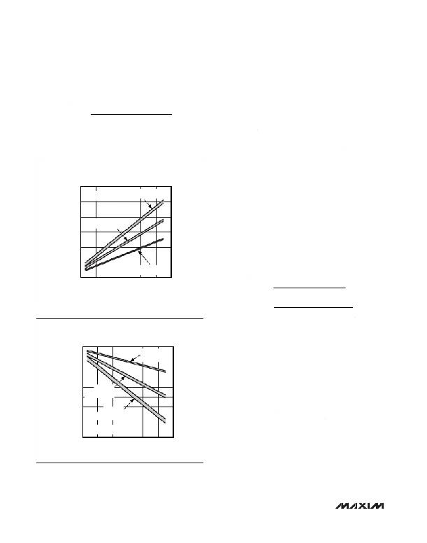
�60�
�50�
�40�
�30�
�20�
�10�
�POSITIVE� CHARGE-PUMP�
�OUTPUT� VOLTAGE� vs.� V� MAIN�
�3-STAGE� CHARGE� PUMP�
�2-STAGE� CHARGE� PUMP�
�1-STAGE� CHARGE� PUMP�
�stages,� V� GOFF� is� the� gate-off� linear-regulator� REG� N�
�output,� V� MAIN� is� the� main� step-up� regulator� output,� V� D�
�is� the� forward-voltage� drop� of� the� charge-pump� diode,�
�and� V� DROPOUT� is� the� dropout� margin� for� the� linear� reg-�
�ulator.� Use� V� DROPOUT� =� 0.3V.�
�The� above� equations� are� derived� based� on� the�
�assumption� that� the� first� stage� of� the� positive� charge�
�pump� is� connected� to� V� MAIN� and� the� first� stage� of� the�
�negative� charge� pump� is� connected� to� ground.�
�Sometimes� fractional� stages� are� more� desirable� for� bet-�
�ter� efficiency.� This� can� be� done� by� connecting� the� first�
�stage� to� V� IN� or� another� available� supply.� If� the� first�
�charge-pump� stage� is� powered� from� V� IN� ,� the� above�
�equations� become:�
�n� POS� =� GON� DROPOUT� IN�
�0�
�2�
�4�
�6�
�8�
�V� MAIN� (V)�
�10�
�12�
�14�
�V� +� V� +� V�
�V� MAIN� ?� 2� � V� D�
�Figure� 8.� Positive� Charge-Pump� Output� Voltage� vs.� V� MAIN�
�n� NEG� =�
�?� V� GOFF� +� V� DROPOUT� +� V� IN�
�V� MAIN� ?� 2� � V� D�
�-0�
�NEGATIVE� CHARGE-PUMP�
�OUTPUT� VOLTAGE� vs.� V� MAIN�
�Flying� Capacitors�
�Increasing� the� flying-capacitor� (C� X� )� value� lowers� the�
�effective� source� impedance� and� increases� the� output-�
�-5�
�-10�
�-15�
�-20�
�-25�
�-30�
�-35�
�-40�
�-45�
�2-STAGE�
�CHARGE� PUMP�
�3-STAGE�
�CHARGE� PUMP�
�V� D� =� 0.3V� TO� 1V�
�1-STAGE�
�CHARGE� PUMP�
�current� capability.� Increasing� the� capacitance� indefinitely�
�has� a� negligible� effect� on� output-current� capability�
�because� the� internal� switch� resistance� and� the� diode�
�impedance� place� a� lower� limit� on� the� source� imped-�
�ance.� A� 0.1μF� ceramic� capacitor� works� well� in� most�
�low-current� applications.� The� flying� capacitor’s� voltage�
�rating� must� exceed� the� following:�
�V� CX� >� n� � V� MAIN�
�where� n� is� the� stage� number� in� which� the� flying� capaci-�
�tor� appears,� and� V� MAIN� is� the� output� voltage� of� the�
�2�
�4�
�6�
�8�
�10�
�12�
�14�
�main� step-up� regulator.�
�V� MAIN� (V)�
�Figure� 9.� Negative� Charge-Pump� Output� Voltage� vs.� V� MAIN�
�22�
�______________________________________________________________________________________�
�相关PDF资料 |
PDF描述 |
|---|---|
| MAX8798ETX+T | IC INTERNAL-SW BOOST REG 36-TQFN |
| MAX8804VETA+T | IC USB/AC ADP CHARGER 8TDFN-EP |
| MAX8804YETA+T | IC USB/AC ADP CHARGER 8-TDFN |
| MAX8805WEWECE+T | IC PWM STEP-DN CONV 650MA 16-WLP |
| MAX8808XETA+T | IC BATT CHRGR 1-CELL LI+ 8TDFN |
相关代理商/技术参数 |
参数描述 |
|---|---|
| MAX8795AEVKIT+ | 功能描述:电源管理IC开发工具 MAX8795A Eval Kit RoHS:否 制造商:Maxim Integrated 产品:Evaluation Kits 类型:Battery Management 工具用于评估:MAX17710GB 输入电压: 输出电压:1.8 V |
| MAX8795AGCJ/V+ | 功能描述:LCD 驱动器 TFT-LCD DC/DC Converter RoHS:否 制造商:Maxim Integrated 数位数量:4.5 片段数量:30 最大时钟频率:19 KHz 工作电源电压:3 V to 3.6 V 最大工作温度:+ 85 C 最小工作温度:- 20 C 封装 / 箱体:PDIP-40 封装:Tube |
| MAX8795AGCJ/V+T | 功能描述:LCD 驱动器 TFT-LCD DC/DC Converter RoHS:否 制造商:Maxim Integrated 数位数量:4.5 片段数量:30 最大时钟频率:19 KHz 工作电源电压:3 V to 3.6 V 最大工作温度:+ 85 C 最小工作温度:- 20 C 封装 / 箱体:PDIP-40 封装:Tube |
| MAX8795AGCJ+ | 功能描述:LCD 驱动器 TFT-LCD DC/DC Converter RoHS:否 制造商:Maxim Integrated 数位数量:4.5 片段数量:30 最大时钟频率:19 KHz 工作电源电压:3 V to 3.6 V 最大工作温度:+ 85 C 最小工作温度:- 20 C 封装 / 箱体:PDIP-40 封装:Tube |
| MAX8795AGCJ+T | 功能描述:LCD 驱动器 TFT-LCD DC/DC Converter RoHS:否 制造商:Maxim Integrated 数位数量:4.5 片段数量:30 最大时钟频率:19 KHz 工作电源电压:3 V to 3.6 V 最大工作温度:+ 85 C 最小工作温度:- 20 C 封装 / 箱体:PDIP-40 封装:Tube |
发布紧急采购,3分钟左右您将得到回复。