- 您现在的位置:买卖IC网 > PDF目录14487 > MAX8833ETJ+ (Maxim Integrated Products)IC REG BUCK ADJ 3A DL 32TQFN PDF资料下载
参数资料
| 型号: | MAX8833ETJ+ |
| 厂商: | Maxim Integrated Products |
| 文件页数: | 7/20页 |
| 文件大小: | 0K |
| 描述: | IC REG BUCK ADJ 3A DL 32TQFN |
| 产品培训模块: | Lead (SnPb) Finish for COTS Obsolescence Mitigation Program |
| 标准包装: | 60 |
| 类型: | 降压(降压) |
| 输出类型: | 可调式 |
| 输出数: | 2 |
| 输出电压: | 0.6 V ~ 3.24 V |
| 输入电压: | 2.35 V ~ 3.6 V |
| PWM 型: | 电压模式 |
| 频率 - 开关: | 1MHz ~ 2MHz |
| 电流 - 输出: | 3A |
| 同步整流器: | 无 |
| 工作温度: | -40°C ~ 85°C |
| 安装类型: | 表面贴装 |
| 封装/外壳: | 32-WFQFN 裸露焊盘 |
| 包装: | 管件 |
| 供应商设备封装: | 32-TQFN-EP(5x5) |
�� �
�
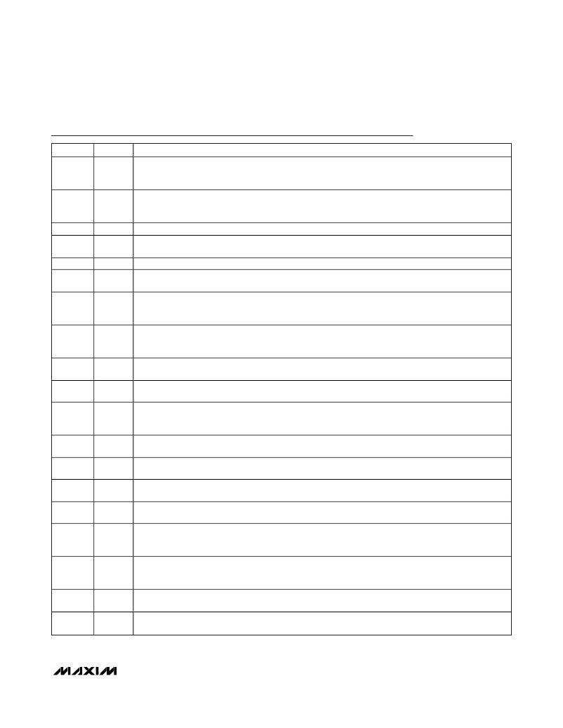
�Dual,� 3A,� 2MHz� Step-Down� Regulator�
�Pin� Description�
�PIN�
�NAME�
�FUNCTION�
�Power-Good� Open-Drain� Output� for� Regulator� 1.� PWRGD1� is� high� impedance� when� V� REFIN� ≥� 0.54V� and�
�1�
�PWRGD1� V� FB1� ≥� 0.9� x� V� REFIN� .� PWRGD1� is� low� when� V� REFIN� <� 0.54V,� EN1� is� low,� V� DD� or� IN1� is� below� UVLO,� the�
�thermal� shutdown� is� activated,� or� when� V� FB1� <� 0.9� x� V� REFIN� .�
�External� Reference� Input� for� Regulator� 1.� Connect� an� external� reference� to� REFIN,� or� connect� REFIN� to� SS1�
�2�
�3�
�4�
�5�
�6�
�7�
�REFIN�
�V� DD�
�GND�
�N.C.�
�VDL�
�FSYNC�
�to� use� the� internal� reference.� REFIN� is� discharged� to� GND� through� 335� Ω� when� EN1� is� low� or� regulator� 1� is�
�shut� down� due� to� a� fault� condition.�
�Supply Voltage. Connect a 10� Ω� resistor from V� DD� to VDL and connect a 0.1μF capacitor from V� DD� to GND.�
�Analog� Ground.� Connect� GND� to� the� analog� ground� plane.� Connect� the� analog� and� power� ground� planes�
�together� at� a� single� point� near� the� IC.�
�No� Connection�
�Supply� Voltage� Input� for� Low-Side� Gate� Drive.� Connect� VDL� to� IN_� or� the� highest� available� supply� voltage�
�less� than� 3.6V.� Connect� a� 1μF� capacitor� from� VDL� to� the� power� ground� plane.�
�Frequency� Set� and� Synchronization.� Connect� a� 4.75k� Ω� to� 20.5k� Ω� resistor� from� FSYNC� to� GND� to� set�
�switching� frequency� or� drive� with� a� 250kHz� to� 2.5MHz� clock� signal� to� synchronize� switching.�
�R� FSYNC� =� (T� -� 0.05μs)� x� (10k� Ω� /0.95μs),� where� T� is� the� oscillator� period.�
�8�
�Power-Good� Open-Drain� Output� for� Regulator� 2.� PWRGD2� is� high� impedance� when� V� SS2� ≥� 0.54V� and� V� FB2�
�PWRGD2� ≥� 0.9� x� V� SS2� .� PWRGD2� is� low� when� V� SS2� <� 0.54V,� EN2� is� low,� V� DD� or� IN2� is� below� UVLO,� the� thermal�
�shutdown� is� activated,� or� when� V� FB2� <� 0.9� x� V� SS2� .�
�9�
�10�
�11�
�12�
�13,� 14�
�15,� 16,� 17�
�18,� 19�
�20�
�21�
�22,� 23�
�24,� 25,� 26�
�SS2�
�FB2�
�COMP2�
�EN2�
�IN2�
�PGND2�
�LX2�
�BST2�
�BST1�
�LX1�
�PGND1�
�Soft-Start� for� Regulator� 2.� Connect� a� capacitor� from� SS2� to� GND� to� set� the� soft-start� time.� See� the� Setting� the� Soft-�
�Start� Time� section.� SS2� is� internally� pulled� low� with� 335� Ω� when� EN2� is� low� or� regulator� 2� is� in� a� fault� condition.�
�Feedback� Input� for� Regulator� 2.� Connect� FB2� to� the� center� of� an� external� resistor-divider� from� the� output� to�
�GND� to� set� the� output� voltage� from� 0.6V� to� 90%� of� V� IN2� .� FB2� is� high� impedance� when� the� IC� is� shut� down.�
�Compensation� for� Regulator� 2.� COMP2� is� the� output� of� the� internal� voltage-error� amplifier.� Connect� external�
�compensation� network� from� COMP2� to� FB2.� See� the� Compensation� Design� section.� COMP2� is� internally�
�pulled� to� GND� when� the� output� is� shut� down.�
�Enable� Input� for� Regulator� 2.� Drive� EN2� high� to� enable� regulator� 2,� or� drive� low� for� shutdown.� For� always-on�
�operation,� connect� EN2� to� V� DD� .�
�Power-Supply� Input� for� Regulator� 2.� The� voltage� range� is� 2.35V� to� 3.6V.� Connect� two� 10μF� and� one� 0.1μF�
�ceramic� capacitors� from� IN2� to� PGND2.�
�Power� Ground� for� Regulator� 2.� Connect� all� PGND_� pins� to� the� power� ground� plane.� Connect� the� power�
�ground� and� analog� ground� planes� together� at� a� single� point� near� the� IC.�
�Inductor� Connection� for� Regulator� 2.� Connect� an� inductor� between� LX2� and� the� regulator� output.� LX2� is� high�
�impedance� when� the� IC� is� shut� down.�
�Bootstrap� Connection� for� Regulator� 2.� Connect� a� 0.1μF� capacitor� from� BST2� to� LX2.� BST2� is� the� supply� for�
�the� high-side� gate� drive.� BST2� is� charged� from� VDL� with� an� internal� pMOS� switch.� In� shutdown,� there� is� an�
�internal� diode� junction� from� LX2� to� BST2� and� from� VDL� to� BST2.�
�Bootstrap� Connection� for� Regulator� 1.� Connect� a� 0.1μF� capacitor� from� BST1� to� LX1.� BST1� is� the� supply� for�
�the� high-side� gate� drive.� BST1� is� charged� from� VDL� with� an� internal� pMOS� switch.� In� shutdown,� there� is� an�
�internal� diode� junction� from� LX1� to� BST1� and� from� VDL� to� BST1.�
�Inductor� Connection� for� Regulator� 1.� Connect� an� inductor� between� LX1� and� the� regulator� output.� LX1� is� high�
�impedance� when� the� IC� is� shut� down.�
�Power� Ground� for� Regulator� 1.� Connect� all� PGND_� pins� to� the� power� ground� plane.� Connect� the� power�
�ground� and� analog� ground� planes� together� at� a� single� point� near� the� IC.�
�_______________________________________________________________________________________�
�7�
�相关PDF资料 |
PDF描述 |
|---|---|
| MAX1708EEE+ | IC REG BST 3.3V/5V/ADJ 5A 16QSOP |
| MAX660ESA+ | IC REG SWITCHD CAP DBL INV 8SOIC |
| MAX1774EEI+ | IC REG BUCK SYNC ADJ DL 28QSOP |
| MAX5033BASA+ | IC REG BUCK 5V 0.5A 8SOIC |
| GCC43DREI | CONN EDGECARD 86POS .100 EYELET |
相关代理商/技术参数 |
参数描述 |
|---|---|
| MAX8833ETJ+ | 功能描述:直流/直流开关调节器 Dual 3A 2MHz Step-Down Regulator RoHS:否 制造商:International Rectifier 最大输入电压:21 V 开关频率:1.5 MHz 输出电压:0.5 V to 0.86 V 输出电流:4 A 输出端数量: 最大工作温度: 安装风格:SMD/SMT 封装 / 箱体:PQFN 4 x 5 |
| MAX8833ETJ+T | 功能描述:直流/直流开关调节器 Dual 3A 2MHz Step-Down Regulator RoHS:否 制造商:International Rectifier 最大输入电压:21 V 开关频率:1.5 MHz 输出电压:0.5 V to 0.86 V 输出电流:4 A 输出端数量: 最大工作温度: 安装风格:SMD/SMT 封装 / 箱体:PQFN 4 x 5 |
| MAX8834YEVKIT+ | 功能描述:LED 照明开发工具 Adaptive Step-Up Converters with 1.5A Flash Driver RoHS:否 制造商:Fairchild Semiconductor 产品:Evaluation Kits 用于:FL7732 核心: 电源电压:120V 系列: 封装: |
| MAX8834YEWP+T | 功能描述:LED照明驱动器 Adaptive Step-Up Converter RoHS:否 制造商:STMicroelectronics 输入电压:11.5 V to 23 V 工作频率: 最大电源电流:1.7 mA 输出电流: 最大工作温度: 安装风格:SMD/SMT 封装 / 箱体:SO-16N |
| MAX8834ZEWP+T | 功能描述:LED照明驱动器 Adaptive Step-Up Converter RoHS:否 制造商:STMicroelectronics 输入电压:11.5 V to 23 V 工作频率: 最大电源电流:1.7 mA 输出电流: 最大工作温度: 安装风格:SMD/SMT 封装 / 箱体:SO-16N |
发布紧急采购,3分钟左右您将得到回复。