- 您现在的位置:买卖IC网 > PDF目录11687 > MAX9218ETM+T (Maxim Integrated Products)IC DESERIALIZER LVDS 48-TQFN PDF资料下载
参数资料
| 型号: | MAX9218ETM+T |
| 厂商: | Maxim Integrated Products |
| 文件页数: | 5/15页 |
| 文件大小: | 0K |
| 描述: | IC DESERIALIZER LVDS 48-TQFN |
| 产品培训模块: | Lead (SnPb) Finish for COTS Obsolescence Mitigation Program |
| 标准包装: | 2,500 |
| 功能: | 解串器 |
| 数据速率: | 700Mbps |
| 输入类型: | LVDS |
| 输出类型: | LVCMOS |
| 输入数: | 1 |
| 输出数: | 27 |
| 电源电压: | 3 V ~ 3.6 V |
| 工作温度: | -40°C ~ 85°C |
| 安装类型: | 表面贴装 |
| 封装/外壳: | 48-WFQFN 裸露焊盘 |
| 供应商设备封装: | 48-TQFN-EP(6x6) |
| 包装: | 带卷 (TR) |
MAX9218
27-Bit, 3MHz-to-35MHz
DC-Balanced LVDS Deserializer
______________________________________________________________________________________
13
Staggered and Transition Time Adjusted
Outputs
RGB_OUT[17:0] are grouped into three groups of six,
with each group switching about 1ns apart in the video
phase
to
reduce
EMI
and
ground
bounce.
CNTL_OUT[8:0] switch during the control phase. Output
transition times are slower in the 3MHz-to-7MHz and
7MHz-to-15MHz ranges and faster in the 15MHz-to-
35MHz range.
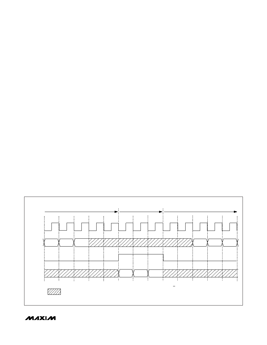
Data Enable Output (DE_OUT)
The MAX9218 deserializes video and control data at dif-
ferent times. Control data is deserialized during the video
blanking time. DE_OUT high indicates that video data is
being deserialized and output on RGB_OUT[17:0].
DE_OUT low indicates that control data is being deserial-
ized and output on CNTL_OUT[8:0]. When outputs are
not being updated, the last data received is latched on
the outputs. Figure 13 shows the DE_OUT timing.
Power-Supply Circuits and Bypassing
There are separate on-chip power domains for digital
circuits and LVTTL/LVCMOS inputs (VCC supply and
GND), outputs (VCCO supply and VCCO GND), PLL
(VCCPLL supply and VCCPLL GND), and the LVDS input
(VCCLVDS supply and VCCLVDS GND). The grounds are
isolated by diode connections. Bypass each VCC,
VCCO, VCCPLL, and VCCLVDS pin with high-frequency,
surface-mount ceramic 0.1F and 0.001F capacitors
in parallel as close to the device as possible, with the
smallest value capacitor closest to the supply pin. The
outputs are powered from VCCO, which accepts a
1.71V to 3.6V supply, allowing direct interface to inputs
with 1.8V to 3.3V logic levels.
Cables and Connectors
Interconnect for LVDS typically has a differential
impedance of 100
Ω. Use cables and connectors that
have matched differential impedance to minimize
impedance discontinuities.
Twisted-pair and shielded twisted-pair cables offer
superior signal quality compared to ribbon cable and
tend to generate less EMI due to magnetic field cancel-
ing effects. Balanced cables pick up noise as common
mode, which is rejected by the LVDS receiver.
Board Layout
Separate the LVTTL/LVCMOS outputs and LVDS inputs
to prevent crosstalk. A four-layer PCB with separate lay-
ers for power, ground, and signals is recommended.
PCLK_OUT
CNTL_OUT
DE_OUT
RGB_OUT
= OUTPUT DATA HELD
PCLK_OUT TIMING SHOWN FOR R/F = HIGH (RISING OUTPUT LATCH EDGE)
CONTROL DATA
VIDEO DATA
Figure 13. Output Timing
相关PDF资料 |
PDF描述 |
|---|---|
| MAX9250ECM+T | IC DESERIALIZER LVDS 48-LQFP |
| MAX9260GCB/V+T | IC DESERIALIZER GMSL 64TQFP |
| MAX9259GCB/V+T | IC SERIALIZER GMSL 64TQFP |
| MAX9217ETM+T | IC SERIALIZER LVDS 48-TQFN |
| VI-B1X-IW-F1 | CONVERTER MOD DC/DC 5.2V 100W |
相关代理商/技术参数 |
参数描述 |
|---|---|
| MAX9218EVKIT+ | 功能描述:界面开发工具 MAX9217/18 Eval Kit RoHS:否 制造商:Bourns 产品:Evaluation Boards 类型:RS-485 工具用于评估:ADM3485E 接口类型:RS-485 工作电源电压:3.3 V |
| MAX921C/D | 功能描述:校验器 IC RoHS:否 制造商:STMicroelectronics 产品: 比较器类型: 通道数量: 输出类型:Push-Pull 电源电压-最大:5.5 V 电源电压-最小:1.1 V 补偿电压(最大值):6 mV 电源电流(最大值):1350 nA 响应时间: 最大工作温度:+ 125 C 安装风格:SMD/SMT 封装 / 箱体:SC-70-5 封装:Reel |
| MAX921C/D DIE | 制造商:Maxim Integrated Products 功能描述: |
| MAX921C/D+ | 功能描述:校验器 IC RoHS:否 制造商:STMicroelectronics 产品: 比较器类型: 通道数量: 输出类型:Push-Pull 电源电压-最大:5.5 V 电源电压-最小:1.1 V 补偿电压(最大值):6 mV 电源电流(最大值):1350 nA 响应时间: 最大工作温度:+ 125 C 安装风格:SMD/SMT 封装 / 箱体:SC-70-5 封装:Reel |
| MAX921CPA | 功能描述:校验器 IC Single Comparator w/1% Precision Ref RoHS:否 制造商:STMicroelectronics 产品: 比较器类型: 通道数量: 输出类型:Push-Pull 电源电压-最大:5.5 V 电源电压-最小:1.1 V 补偿电压(最大值):6 mV 电源电流(最大值):1350 nA 响应时间: 最大工作温度:+ 125 C 安装风格:SMD/SMT 封装 / 箱体:SC-70-5 封装:Reel |
发布紧急采购,3分钟左右您将得到回复。