- 您现在的位置:买卖IC网 > PDF目录2089 > MAX9315EUP+T (Maxim Integrated Products)IC CLK/DATA BUFF MUX 2:5 20TSSOP PDF资料下载
参数资料
| 型号: | MAX9315EUP+T |
| 厂商: | Maxim Integrated Products |
| 文件页数: | 4/11页 |
| 文件大小: | 0K |
| 描述: | IC CLK/DATA BUFF MUX 2:5 20TSSOP |
| 产品培训模块: | Lead (SnPb) Finish for COTS Obsolescence Mitigation Program |
| 标准包装: | 2,500 |
| 类型: | 扇出缓冲器(分配),多路复用器,数据 |
| 电路数: | 1 |
| 比率 - 输入:输出: | 2:5 |
| 差分 - 输入:输出: | 是/是 |
| 输入: | HSTL,LVECL,LVPECL |
| 输出: | LVECL,LVPECL |
| 频率 - 最大: | 1.5GHz |
| 电源电压: | 2.25 V ~ 3.8 V |
| 工作温度: | -40°C ~ 85°C |
| 安装类型: | 表面贴装 |
| 封装/外壳: | 20-TSSOP(0.173",4.40mm 宽) |
| 供应商设备封装: | 20-TSSOP |
| 包装: | 带卷 (TR) |
MAX9315
1:5 Differential LVPECL/LVECL/HSTL
Clock and Data Driver
2
_______________________________________________________________________________________
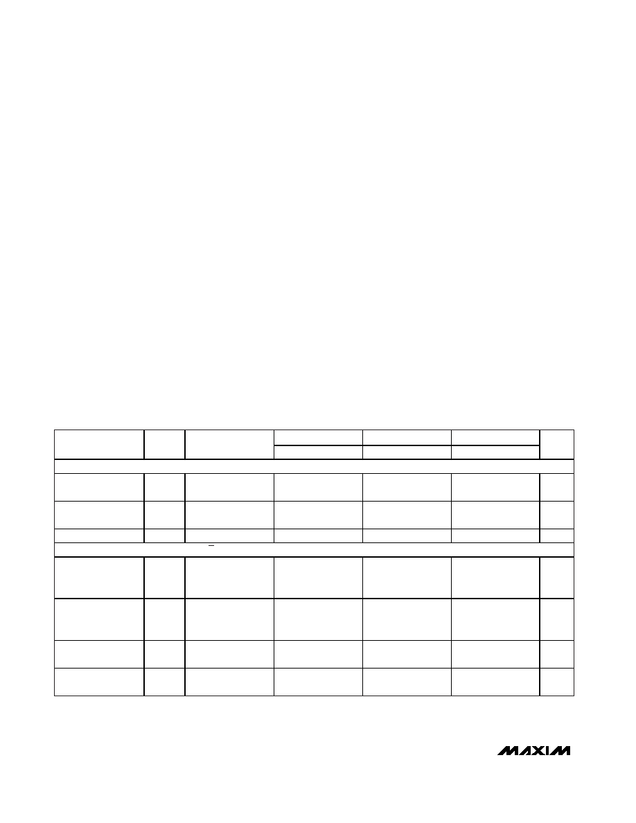
ABSOLUTE MAXIMUM RATINGS
DC ELECTRICAL CHARACTERISTICS
(VCC - VEE = 2.375V to 3.8V, outputs loaded with 50
±1% to VCC - 2V, SEL = high or low, EN = low, unless otherwise noted. Typical
values are at VCC - VEE = +3.3V, VIHD = VCC - 1V, VILD = VCC - 1.5V.) (Notes 1, 2, 3)
Stresses beyond those listed under “Absolute Maximum Ratings” may cause permanent damage to the device. These are stress ratings only, and functional
operation of the device at these or any other conditions beyond those indicated in the operational sections of the specifications is not implied. Exposure to
absolute maximum rating conditions for extended periods may affect device reliability.
VCC - VEE...............................................................................4.1V
Inputs (CLK_, CLK_, SEL, EN)
to VEE ...........................................(VEE - 0.3V) to (VCC + 0.3V)
CLK_ to CLK_ ....................................................................±3.0V
Continuous Output Current .................................................50mA
Surge Output Current........................................................100mA
VBB Sink/Source Current ...............................................±0.65mA
Continuous Power Dissipation (TA = +70°C)
Single-Layer PC Board
20-Pin TSSOP (derate 7.69mW/°C above +70°C) .......615mW
Multilayer PC Board
20-Pin TSSOP (derate 10.9mW/°C above +70°C) .......879mW
Junction-to-Ambient Thermal Resistance in Still Air
Single-Layer PC Board
20-Pin TSSOP .........................................................+130°C/W
Multilayer PC Board
20-Pin TSSOP ...........................................................+91°C/W
Junction-to-Ambient Thermal Resistance with 500LFPM
Airflow Single-Layer PC Board
20-Pin TSSOP ..........................................................+9.6°C/W
Junction-to-Case Thermal Resistance
20-Pin TSSOP ............................................................+20°C/W
Operating Temperature Range ...........................-40°C to +85°C
Junction Temperature ......................................................+150°C
Storage Temperature Range .............................-65°C to +150°C
ESD Protection
Human Body Model (Inputs and Outputs) .......................
≥2kV
Soldering Temperature (10s) ...........................................+300°C
-40
°C
+25
°C
+85
°C
PARAMETER
SYMBOL
CONDITIONS
MIN
TYP
MAX
MIN
TYP
MAX
MIN
TYP
MAX
UNITS
SINGLE-ENDED INPUTS (SEL,
EN)
Input High Voltage
VIH
VCC -
1.225
VCC
VCC -
1.225
VCC
VCC -
1.225
VCC
V
Input Low Voltage
VIL
VEE
VCC -
1.625
VEE
VCC -
1.625
VEE
VCC -
1.625
V
Input Current
IIN
VIH(MAX), VIL(MIN)
-500
500
-500
500
-500
500
A
DIFFERENTIAL INPUTS (CLK_,
CLK_)
Single-Ended Input
High Voltage
(Note 4)
VIH
VBB connected to
CLK_, Figure 1
VCC -
1.225
VCC
VCC -
1.225
VCC
VCC -
1.225
VCC
V
Single-Ended Input
Low Voltage
(Note 4)
VIL
VBB connected to
CLK_, Figure 1
VEE
VCC -
1.625
VEE
VCC -
1.625
VEE
VCC -
1.625
V
High Voltage of
Differential Input
VIHD
VEE +
1.2
VCC
VEE +
1.2
VCC
VEE +
1.2
VCC
V
Low Voltage of
Differential Input
VILD
VEE
VCC -
0.1
VEE
VCC -
0.1
VEE
VCC -
0.1
V
相关PDF资料 |
PDF描述 |
|---|---|
| MAX9316EWP+T | IC CLOCK BUFFER MUX 2:5 20-SOIC |
| MAX9320ESA+T | IC CLOCK BUFFER 2:2 3GHZ 8-SOIC |
| MAX9321EUA+T | IC CLOCK/DATA DRIVER 1:1 8-UMAX |
| MAX9325EQI+T | IC CLK/DATA BUFF MUX 2:8 28-PLCC |
| MAX934ESE+ | IC COMPARATOR W/REF 16-SOIC |
相关代理商/技术参数 |
参数描述 |
|---|---|
| MAX9315EUP-TG068 | 制造商:Maxim Integrated Products 功能描述:1:5 DIFFERENTIAL LVPECL/LVECL/HSTL CLOCK AND - Rail/Tube |
| MAX9315EVKIT | 功能描述:时钟驱动器及分配 Evaluation Kit for the MAX9315 MAX9316 RoHS:否 制造商:Micrel 乘法/除法因子:1:4 输出类型:Differential 最大输出频率:4.2 GHz 电源电压-最大: 电源电压-最小:5 V 最大工作温度:+ 85 C 封装 / 箱体:SOIC-8 封装:Reel |
| MAX9316AEWP | 功能描述:时钟驱动器及分配 RoHS:否 制造商:Micrel 乘法/除法因子:1:4 输出类型:Differential 最大输出频率:4.2 GHz 电源电压-最大: 电源电压-最小:5 V 最大工作温度:+ 85 C 封装 / 箱体:SOIC-8 封装:Reel |
| MAX9316AEWP-T | 功能描述:时钟驱动器及分配 RoHS:否 制造商:Micrel 乘法/除法因子:1:4 输出类型:Differential 最大输出频率:4.2 GHz 电源电压-最大: 电源电压-最小:5 V 最大工作温度:+ 85 C 封装 / 箱体:SOIC-8 封装:Reel |
| MAX9316EUP | 制造商:Maxim Integrated Products 功能描述:1:5 DIFFERENTIAL LVPECL/LVECL/HSTL CLOCK AND - Rail/Tube |
发布紧急采购,3分钟左右您将得到回复。