- 您现在的位置:买卖IC网 > PDF目录8679 > MAX9325EQI+ (Maxim Integrated Products)IC CLK/DATA BUFF MUX 2:8 28-PLCC PDF资料下载
参数资料
| 型号: | MAX9325EQI+ |
| 厂商: | Maxim Integrated Products |
| 文件页数: | 12/12页 |
| 文件大小: | 0K |
| 描述: | IC CLK/DATA BUFF MUX 2:8 28-PLCC |
| 产品培训模块: | Lead (SnPb) Finish for COTS Obsolescence Mitigation Program |
| 标准包装: | 39 |
| 类型: | 扇出缓冲器(分配),多路复用器,数据 |
| 电路数: | 1 |
| 比率 - 输入:输出: | 2:8 |
| 差分 - 输入:输出: | 是/是 |
| 输入: | HSTL,LVECL,LVPECL |
| 输出: | LVECL,LVPECL |
| 频率 - 最大: | 700MHz |
| 电源电压: | 2.375 V ~ 3.8 V |
| 工作温度: | -40°C ~ 85°C |
| 安装类型: | 表面贴装 |
| 封装/外壳: | 28-LCC(J 形引线) |
| 供应商设备封装: | 28-PLCC(11.51x11.51) |
| 包装: | 管件 |
MAX9325
2:8 Differential LVPECL/LVECL/HSTL Clock and
Data Driver
_______________________________________________________________________________________
9
Detailed Description
The MAX9325 low-skew, 2:8 differential driver features
extremely low output-to-output skew (50ps max) and
part-to-part skew (225ps max). These features make the
device ideal for clock and data distribution across a
backplane or board. The device selects one of the two
differential HSTL or LVECL/LVPECL inputs, and repeats
them at eight differential outputs. Outputs are compati-
ble with LVECL and LVPECL, and can directly drive 50
terminated transmission lines.
A 2:1 mux selects between the two differential inputs,
CLK0, CLK0 and CLK1, CLK1. The 2:1 mux is switched
by the single-ended CLK_SEL input. A logic low selects
the CLK0, CLK0 input. A logic high selects the CLK1,
CLK1 input. The logic threshold for CLK_SEL is set by
an internal VBB voltage reference. The selected input is
reproduced at eight differential outputs at speeds up to
700MHz.
The differential inputs can be configured to accept a
single-ended signal when the unused complementary
input is connected to the on-chip reference output volt-
age (VBB). A single-ended input of at least VBB ±95mV
or a differential input of at least 95mV switches the out-
puts to the VOH and VOL levels specified in the DC
Electrical Characteristics. The maximum magnitude of
the differential input from CLK_ to CLK_ is ±3.0V or
±(VCC - VEE), whichever is less. This limit also applies
to the difference between a single-ended input and any
reference voltage input.
The single-ended CLK_SEL input has a 75k pulldown
to VEE that selects the default input, CLK0, CLK0, when
CLK_SEL is left open or at VEE. All the differential inputs
have 105k pulldowns to VEE. Internal pulldowns and a
fail-safe circuit ensure differential low default outputs
when the inputs are left open or at VEE.
Specifications for the high and low voltages of a differ-
ential input (VIHD and VILD) and the differential input
voltage (VIHD - VILD) apply simultaneously.
For interfacing to differential HSTL and LVPECL signals,
these devices operate over a +2.375V to +3.8V supply
range, allowing high-performance clock or data distrib-
ution in systems with a nominal +2.5V or +3.3V supply.
For differential LVECL operation, these devices operate
from a -2.375V to -3.8V supply.
Single-Ended Operation
CLK_SEL is a single-ended input with the input threshold
internally set to VBB, and can be driven to VCC or VEE or
by a single-ended LVPECL/LVECL signal. The CLK_,
CLK_ are differential inputs but can be configured to
accept single-ended inputs when operating at supply
voltages greater than 2.58V. The recommended supply
voltage for single-ended operation is 3.0V to 3.8V. A dif-
OR
VBB
tPLH
tPHL
VOH - VOL
Q_
CLK_ WHEN CLK_ = VBB
VOH
VIL
VIH
VOL
CLK_ WHEN CLK_ = VBB
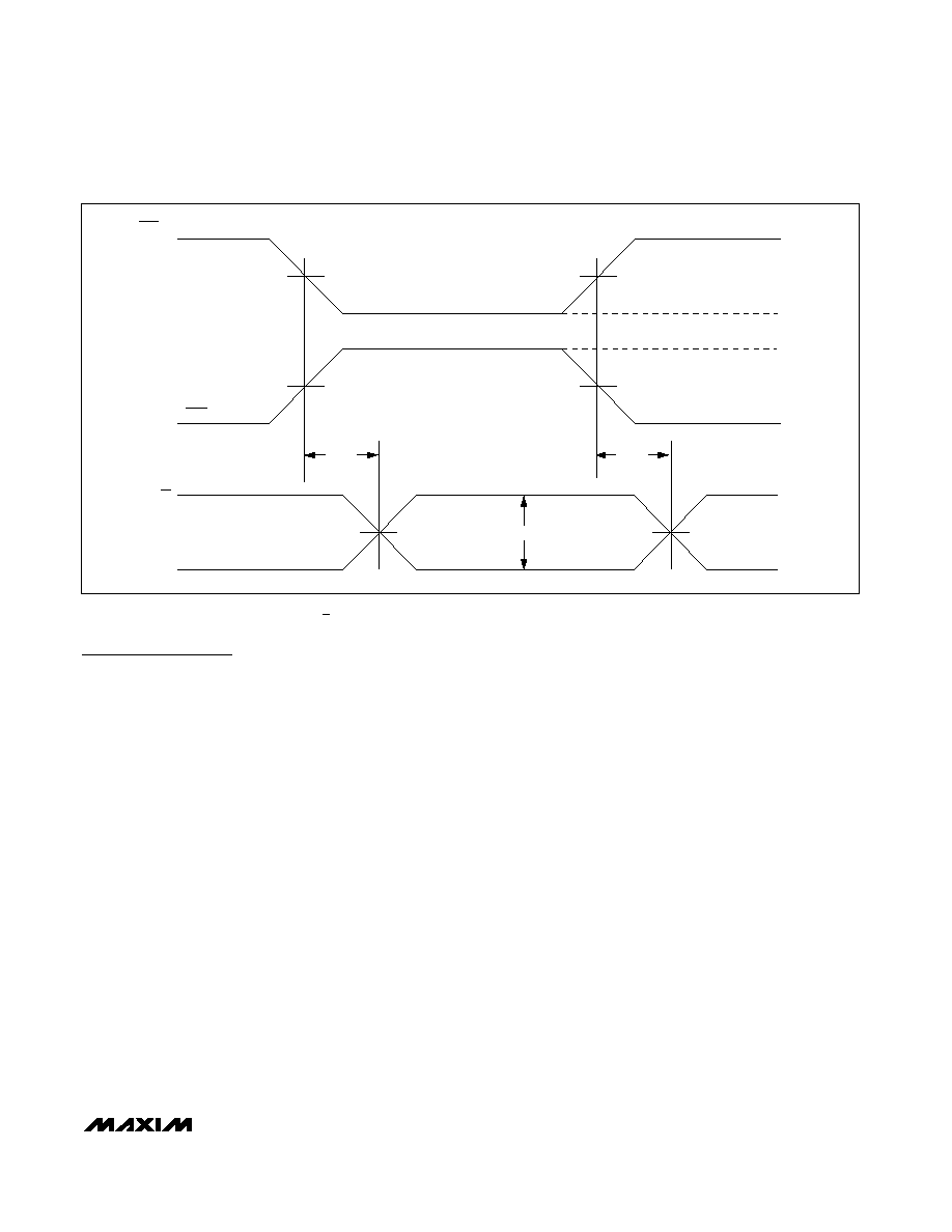
Figure 3. Single-Ended Input (CLK_, CLK_) to Output (Q_, Q_) Delay Timing Diagram
相关PDF资料 |
PDF描述 |
|---|---|
| V300A24H500B2 | CONVERTER MOD DC/DC 24V 500W |
| VE-J5Z-MY | CONVERTER MOD DC/DC 2V 20W |
| V300A24H500B | CONVERTER MOD DC/DC 24V 500W |
| MAX9312ETJ+T | IC CLK/DATA BUFF 1:5 3GHZ 32TQFN |
| V300A15H500BG3 | CONVERTER MOD DC/DC 15V 500W |
相关代理商/技术参数 |
参数描述 |
|---|---|
| MAX9325EQI+ | 功能描述:时钟驱动器及分配 LVPECL/LVECL/HSTL Clock & Data Driver RoHS:否 制造商:Micrel 乘法/除法因子:1:4 输出类型:Differential 最大输出频率:4.2 GHz 电源电压-最大: 电源电压-最小:5 V 最大工作温度:+ 85 C 封装 / 箱体:SOIC-8 封装:Reel |
| MAX9325EQI+T | 功能描述:时钟驱动器及分配 LVPECL/LVECL/HSTL Clock & Data Driver RoHS:否 制造商:Micrel 乘法/除法因子:1:4 输出类型:Differential 最大输出频率:4.2 GHz 电源电压-最大: 电源电压-最小:5 V 最大工作温度:+ 85 C 封装 / 箱体:SOIC-8 封装:Reel |
| MAX9325EVKIT | 制造商:Maxim Integrated Products 功能描述:2:8 DIFFERENTIAL LVPECL/LVECL/HSTL CLOCK AND DATA DRIVER - Boxed Product (Development Kits) |
| MAX9326EGI | 制造商:Rochester Electronics LLC 功能描述: 制造商:Maxim Integrated Products 功能描述: |
| MAX9326EQI | 制造商:Maxim Integrated Products 功能描述:1:9 DIFFERENTIAL LVPECL/LVECL/HSTL CLOCK AND - Rail/Tube |
发布紧急采购,3分钟左右您将得到回复。