- 您现在的位置:买卖IC网 > PDF目录8679 > MAX9325EQI+ (Maxim Integrated Products)IC CLK/DATA BUFF MUX 2:8 28-PLCC PDF资料下载
参数资料
| 型号: | MAX9325EQI+ |
| 厂商: | Maxim Integrated Products |
| 文件页数: | 2/12页 |
| 文件大小: | 0K |
| 描述: | IC CLK/DATA BUFF MUX 2:8 28-PLCC |
| 产品培训模块: | Lead (SnPb) Finish for COTS Obsolescence Mitigation Program |
| 标准包装: | 39 |
| 类型: | 扇出缓冲器(分配),多路复用器,数据 |
| 电路数: | 1 |
| 比率 - 输入:输出: | 2:8 |
| 差分 - 输入:输出: | 是/是 |
| 输入: | HSTL,LVECL,LVPECL |
| 输出: | LVECL,LVPECL |
| 频率 - 最大: | 700MHz |
| 电源电压: | 2.375 V ~ 3.8 V |
| 工作温度: | -40°C ~ 85°C |
| 安装类型: | 表面贴装 |
| 封装/外壳: | 28-LCC(J 形引线) |
| 供应商设备封装: | 28-PLCC(11.51x11.51) |
| 包装: | 管件 |
MAX9325
2:8 Differential LVPECL/LVECL/HSTL Clock and
Data Driver
10
______________________________________________________________________________________
ferential input is configured for single-ended operation
by connecting the on-chip reference voltage, VBB, to an
unused complementary input as a reference. For exam-
ple, the differential CLK0, CLK0 input is converted to a
noninverting, single-ended input by connecting VBB to
CLK0 and connecting the single-ended input to CLK0.
Similarly, an inverting input is obtained by connecting
VBB to CLK0 and connecting the single-ended input to
CLK0. With a differential input configured as single-
ended (using VBB), the single-ended input can be driven
to VCC or VEE or with a single-ended LVPECL/LVECL
signal.
When configuring a differential input as a single-ended
input, a user must ensure that the supply voltage (VCC -
VEE) is greater than 2.58V. This is because the input
high minimum level must be at (VEE + 1.2V) or higher
for proper operation. The reference voltage VBB must
be at least (VEE + 1.2V) or higher for the same reason
because it becomes the high-level input when the other
single-ended input swings below it. The minimum VBB
output for the MAX9325 is (VCC - 1.38V). Substituting
the minimum VBB output for (VBB = VEE + 1.2V) results
in a minimum supply (VCC - VEE) of 2.58V. Rounding up
to standard supplies gives the single-ended operating
supply ranges (VCC - VEE ) of 3.0V to 3.8V for the
MAX9325.
When using the VBB reference output, bypass it with a
0.01F ceramic capacitor to VCC. If not used, leave it
open. The VBB reference can source or sink 0.5mA,
which is sufficient to drive two inputs.
Applications Information
Output Termination
Terminate the outputs through 50 to (VCC - 2V) or use
equivalent Thevenin terminations. Terminate each Q and
Q output with identical termination on each for low output
distortion. When a single-ended signal is taken from the
differential output, terminate both Q_ and Q_.
Ensure that output currents do not exceed the current
limits as specified in the Absolute Maximum Ratings
table. Under all operating conditions, the device’s total
thermal limits should be observed.
Supply Bypassing
Bypass each VCC to VEE with high-frequency surface-
mount ceramic 0.1F and 0.01F capacitors. Place the
capacitors as close to the device as possible with the
0.01F capacitor closest to the device pins.
Use multiple vias when connecting the bypass capaci-
tors to ground. When using the VBB reference output,
bypass it with a 0.01F ceramic capacitor to VCC. If the
VBB reference is not used, it can be left open.
Traces
Circuit board trace layout is very important to maintain
the signal integrity of high-speed differential signals.
Maintaining integrity is accomplished in part by reduc-
ing signal reflections and skew, and increasing com-
mon-mode noise immunity.
Signal reflections are caused by discontinuities in the
50 characteristic impedance of the traces. Avoid dis-
continuities by maintaining the distance between differ-
ential traces, not using sharp corners or using vias.
Maintaining distance between the traces also increases
common-mode noise immunity. Reducing signal skew
is accomplished by matching the electrical length of
the differential traces.
Exposed-Pad Package
The 28-lead QFN package (MAX9325EGI) has the
exposed paddle on the bottom of the package that pro-
vides the primary heat removal path from the IC to the
PC board, as well as excellent electrical grounding to
the PC board.
The MAX9325EGI’s exposed pad is
internally connected to VEE. Do not connect the
exposed pad to a separate circuit ground plane
unless VEE and the circuit ground are the same.
Chip Information
TRANSISTOR COUNT: 1030
PROCESS: Bipolar
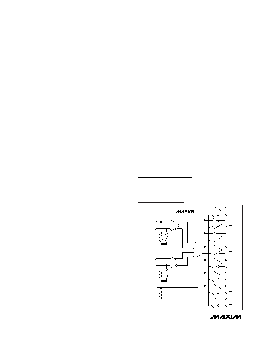
Q0
Q1
Q2
Q3
Q4
Q5
0
1
Q5
Q6
Q7
VEE
CLK1
CLK_SEL
CLK1
105k
75k
VEE
CLK0
105k
MAX9325
Functional Diagram
相关PDF资料 |
PDF描述 |
|---|---|
| V300A24H500B2 | CONVERTER MOD DC/DC 24V 500W |
| VE-J5Z-MY | CONVERTER MOD DC/DC 2V 20W |
| V300A24H500B | CONVERTER MOD DC/DC 24V 500W |
| MAX9312ETJ+T | IC CLK/DATA BUFF 1:5 3GHZ 32TQFN |
| V300A15H500BG3 | CONVERTER MOD DC/DC 15V 500W |
相关代理商/技术参数 |
参数描述 |
|---|---|
| MAX9325EQI+ | 功能描述:时钟驱动器及分配 LVPECL/LVECL/HSTL Clock & Data Driver RoHS:否 制造商:Micrel 乘法/除法因子:1:4 输出类型:Differential 最大输出频率:4.2 GHz 电源电压-最大: 电源电压-最小:5 V 最大工作温度:+ 85 C 封装 / 箱体:SOIC-8 封装:Reel |
| MAX9325EQI+T | 功能描述:时钟驱动器及分配 LVPECL/LVECL/HSTL Clock & Data Driver RoHS:否 制造商:Micrel 乘法/除法因子:1:4 输出类型:Differential 最大输出频率:4.2 GHz 电源电压-最大: 电源电压-最小:5 V 最大工作温度:+ 85 C 封装 / 箱体:SOIC-8 封装:Reel |
| MAX9325EVKIT | 制造商:Maxim Integrated Products 功能描述:2:8 DIFFERENTIAL LVPECL/LVECL/HSTL CLOCK AND DATA DRIVER - Boxed Product (Development Kits) |
| MAX9326EGI | 制造商:Rochester Electronics LLC 功能描述: 制造商:Maxim Integrated Products 功能描述: |
| MAX9326EQI | 制造商:Maxim Integrated Products 功能描述:1:9 DIFFERENTIAL LVPECL/LVECL/HSTL CLOCK AND - Rail/Tube |
发布紧急采购,3分钟左右您将得到回复。