- 您现在的位置:买卖IC网 > PDF目录16982 > MAXADCLITE# (Maxim Integrated Products)KIT EVALUATION FOR MAX11645 PDF资料下载
参数资料
| 型号: | MAXADCLITE# |
| 厂商: | Maxim Integrated Products |
| 文件页数: | 6/22页 |
| 文件大小: | 0K |
| 描述: | KIT EVALUATION FOR MAX11645 |
| 产品培训模块: | Obsolescence Mitigation Program |
| 标准包装: | 1 |
| ADC 的数量: | 1 |
| 位数: | 12 |
| 采样率(每秒): | 94.4k |
| 数据接口: | USB |
| 输入范围: | ±VREF/2 |
| 工作温度: | -40°C ~ 85°C |
| 已用 IC / 零件: | MAX11645 |
| 已供物品: | 板,软件 |
MAX11644/MAX11645
Low-Power, 1-/2-Channel, I2C, 12-Bit ADCs
in Ultra-Tiny 1.9mm x 2.2mm Package
14
______________________________________________________________________________________
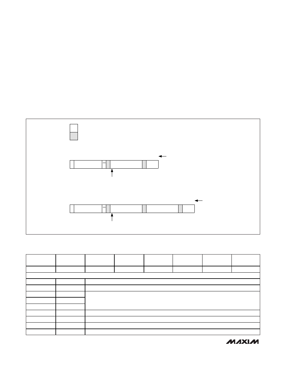
Configuration/Setup Bytes (Write Cycle)
A write cycle begins with the bus master issuing a
START condition followed by seven address bits
(Figure 7) and a write bit (R/W = 0). If the address byte
is successfully received, the MAX11644/MAX11645
(slave) issues an acknowledge. The master then writes
to the slave. The slave recognizes the received byte as
the set-up byte (Table 1) if the most significant bit
(MSB) is 1. If the MSB is 0, the slave recognizes that
byte as the configuration byte (Table 2). The master
can write either one or two bytes to the slave in any
order (setup byte, then configuration byte; configura-
tion byte, then setup byte; setup byte or configuration
byte only; Figure 9). If the slave receives a byte suc-
cessfully, it issues an acknowledge. The master ends
the write cycle by issuing a STOP condition or a repeat-
ed START condition. When operating in HS mode, a
STOP condition returns the bus into F/S mode (see the
HS Mode section).
B) TWO-BYTE WRITE CYCLE
SLAVE TO MASTER
MASTER TO SLAVE
S
1
SLAVE ADDRESS
A
71 1
W
SETUP OR
CONFIGURATION BYTE
SETUP OR
CONFIGURATION BYTE
8
P OR Sr
1
A
1
MSB DETERMINES WHETHER
SETUP OR CONFIGURATION BYTE
S
1
SLAVE ADDRESS
A
71 1
W
SETUP OR
CONFIGURATION BYTE
8
P OR Sr
1
A
1
MSB DETERMINES WHETHER
SETUP OR CONFIGURATION BYTE
A
1
8
A) ONE-BYTE WRITE CYCLE
NUMBER OF BITS
Figure 9. Write Cycle
BIT 7
(MSB)
BIT 6
BIT 5
BIT 4
BIT 3
BIT 2
BIT 1
BIT 0
(LSB)
REG
SEL2
SEL1
SEL0
CLK
BIP/UNI
RST
X
BIT
NAME
DESCRIPTION
7
REG
Register bit. 1 = setup byte, 0 = configuration byte (Table 2).
6
SEL2
5
SEL1
4
SEL0
Three bits select the reference voltage (Table 6).
Default to 000 at power-up.
3
CLK
1 = external clock, 0 = internal clock. Defaults to 0 at power-up.
2
BIP/UNI
1 = bipolar, 0 = unipolar. Defaults to 0 at power-up (see the Unipolar/Bipolar section).
1
RST
1 = no action, 0 = resets the configuration register to default. Setup register remains unchanged.
0
X
Don’t-care bit. This bit can be set to 1 or 0.
Table 1. Setup Byte Format
相关PDF资料 |
PDF描述 |
|---|---|
| EMM08DTBH | CONN EDGECARD 16POS R/A .156 SLD |
| FPF2110 | IC SWITCH LOAD FULL FUNC SOT23-5 |
| EMM08DTBD | CONN EDGECARD 16POS R/A .156 SLD |
| HBC10DRAN | CONN EDGECARD 20POS R/A .100 SLD |
| EEM25DTAT | CONN EDGECARD 50POS R/A .156 SLD |
相关代理商/技术参数 |
参数描述 |
|---|---|
| MAXADCLITE# | 功能描述:数据转换 IC 开发工具 MAX11645 Eval Kit RoHS:否 制造商:Texas Instruments 产品:Demonstration Kits 类型:ADC 工具用于评估:ADS130E08 接口类型:SPI 工作电源电压:- 6 V to + 6 V |
| MAXADCLITE+ | 功能描述:数据转换 IC 开发工具 MAX11645 Eval Kit RoHS:否 制造商:Texas Instruments 产品:Demonstration Kits 类型:ADC 工具用于评估:ADS130E08 接口类型:SPI 工作电源电压:- 6 V to + 6 V |
| MAX-B550 | 制造商:SAMSUNG 制造商全称:Samsung semiconductor 功能描述:THREE-CD CHANGER MINI-COMPACT SYSTEM CD-R/RW PLAYBACK |
| MAX-B570 | 制造商:SAMSUNG 制造商全称:Samsung semiconductor 功能描述:THREE-CD CHANGER MINI-COMPACT SYSTEM CD-R/RW PLAYBACK |
| MAXC001 | 制造商:Maxim Integrated Products 功能描述: |
发布紧急采购,3分钟左右您将得到回复。