- 您现在的位置:买卖IC网 > PDF目录378653 > MC100E1651FN (Motorola, Inc.) DUAL ECL OUTPUT COMPARATOR WITH LATCH PDF资料下载
参数资料
| 型号: | MC100E1651FN |
| 厂商: | Motorola, Inc. |
| 英文描述: | DUAL ECL OUTPUT COMPARATOR WITH LATCH |
| 中文描述: | 双ECL锁存输出比较器 |
| 文件页数: | 3/7页 |
| 文件大小: | 133K |
| 代理商: | MC100E1651FN |
MC10E1651
2–3
MOTOROLA
ECLinPS and ECLinPS Lite
DL140 — Rev 4
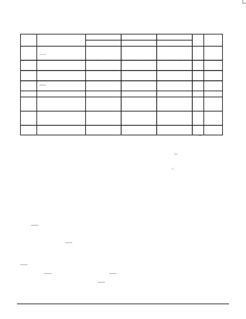
AC CHARACTERISTICS
(VEE = –5.2 V
±
5%; VCC = +5.0 V
±
5%)
0
°
C
25
°
C
85
°
C
Symbol
Characteristic
Min
Typ
Max
Min
Typ
Max
Min
Typ
Max
Unit
Condition
tPLH
tPHL
Propagation Delay to Output
V to Q
LEN to Q
600
400
750
575
900
750
625
400
775
575
925
750
700
500
850
650
1050
850
ps
1
ts
Setup Time
V
450
300
450
300
550
350
ps
th
Enable Hold Time
V
–50
–250
–50
–250
–100
–250
ps
tpw
Minimum Pulse Width
LEN
400
400
400
ps
tskew
TDE
Within Device Skew
15
15
15
ps
2
Delay Dispersion
(ECL Levels)
100
60
ps
3, 4
3, 5
TDL
Delay Dispersion
(TTL Levels)
350
100
ps
6, 7
5, 6
tr
tf
Rise/Fall Times
20-80%
225
325
475
225
325
475
250
375
500
ps
1. The propagation delay is measured from the crosspoint of the input signal and the threshold value to the crosspoint of the Q and Q output signals.
For propagation delay measurements the threshold level (VTHR) is centered about an 850mV input logic swing with a slew rate of 0.75 V/NS.
There is an insignificant change in the propagation delay over the input common mode range.
2. tskew is the propagation delay skew between comparator A and comparator B for a particular part under identical input conditions.
3. Refer to figure 4 and note that the input is at 850mV ECL levels with the input threshold range between the 20% and 80% points. The delay
is measured from the crosspoint of the input signal and the threshold value to the crosspoint of the Q and Q output signals.
4. The slew rate is 0.25 V/NS for input rising edges.
5. The slew rate is 0.75 V/NS for input rising edges.
6. Refer to Figure 5 and note that the input is at 2.5 V TTL levels with the input threshold range between the 20% and 80% points. The delay is
measured from the crosspoint of the input signal and the threshold value to the crosspoint of the Q and Q output signals.
7. The slew rate is 0.3 V/NS for input rising edges.
APPLICATIONS INFORMATION
The timing diagram (Figure 3) is presented to illustrate the
MC10E1651’s compare and latch features. When the signal
on the LEN pin is at a logic high level, the device is operating
in the “compare mode,” and the signal on the input arrives at
the output after a nominal propagation delay (tPHL, tPLH). The
input signal must be asserted for a time, ts, prior to the
negative going transition on LEN and held for a time, th, after
the LEN transition. After time th, the latch is operating in the
“latch mode,” thus transitions on the input do not appear at
the output. The device continues to operate in the “latch
mode” until the latch is asserted once again. Moreover, the
LEN pulse must meet the minimum pulse width (tpw)
requirement to effect the correct input-output relationship.
Note that the LEN waveform in Figure 3 shows the LEN
signal swinging around a reference labeled VBBINT; this
waveform emphasizes the requirement that LEN follow
typical ECL 10KH logic levels because VBBINT is the
internally generated reference level, hence is nominally at
the ECL VBB level.
Finally, VOD is the input voltage overdrive and represents
the voltage level beyond the threshold level (VTHR) to which
the input is driven. As an example, if the threshold level is set
on one of the comparator inputs as 80mV and the input signal
swing on the complementary input is from zero to 100mV, the
positive going overdrive would be 20mV and the negative
going overdrive would be 80mV. The result of differing
overdrive levels is that the devices have shorter propagation
delays with greater overdrive because the threshold level is
crossed sooner than the case of lower overdrive levels.
Typically, semiconductor manufactures refer to the threshold
voltage as the input offset voltage (VOS) since the threshold
voltage is the sum of the externally supplied reference
voltage and inherent device offset voltage.
相关PDF资料 |
PDF描述 |
|---|---|
| MC100EL15D | 1:4 Clock Distribution Chip |
| MC100EP221FA | LOW-VOLTAGE 1:20 DIFFERENTIAL ECL/PECL CLOCK DRIVER |
| MC100LVEL01D | 4-Input OR/NOR |
| MC100LVEL05D | 2-Input Differential AND/NAND |
| MC100LVEL11D | Low Voltage 1:2 Differential Fanout Buffer |
相关代理商/技术参数 |
参数描述 |
|---|---|
| MC100E166 | 制造商:ONSEMI 制造商全称:ON Semiconductor 功能描述:9-BIT MAGNITUDE COMPARATOR |
| MC100E166FN | 制造商:MOTOROLA 制造商全称:Motorola, Inc 功能描述:9-BIT MAGNITUDE COMPARATOR |
| MC100E166FNR2 | 制造商:ONSEMI 制造商全称:ON Semiconductor 功能描述:5V ECL 9-Bit Magnitude Comparator |
| MC100E166FNR2G | 制造商:ONSEMI 制造商全称:ON Semiconductor 功能描述:5V ECL 9-Bit Magnitude Comparator |
| MC100E167 | 制造商:ONSEMI 制造商全称:ON Semiconductor 功能描述:6-BIT 2:1 MUX-REGISTER |
发布紧急采购,3分钟左右您将得到回复。