参数资料
| 型号: | MC100EP14DT |
| 厂商: | ON Semiconductor |
| 文件页数: | 5/9页 |
| 文件大小: | 0K |
| 描述: | IC CLK BUFF MUX 2:5 2GHZ 20TSSOP |
| 标准包装: | 75 |
| 系列: | 100EP |
| 类型: | 扇出缓冲器(分配),多路复用器 |
| 电路数: | 1 |
| 比率 - 输入:输出: | 2:5 |
| 差分 - 输入:输出: | 是/是 |
| 输入: | ECL,HSTL,PECL |
| 输出: | ECL,PECL |
| 频率 - 最大: | 2GHz |
| 电源电压: | 3 V ~ 5.5 V |
| 工作温度: | -40°C ~ 85°C |
| 安装类型: | 表面贴装 |
| 封装/外壳: | 20-TSSOP(0.173",4.40mm 宽) |
| 供应商设备封装: | 20-TSSOP |
| 包装: | 管件 |
| 其它名称: | MC100EP14DTOS |
MC100EP14
http://onsemi.com
5
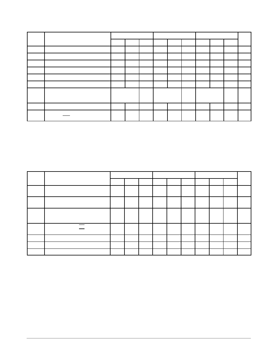
Symbol
Characteristic
40°C
25°C
85°C
Unit
Min
Typ
Max
Min
Typ
Max
Min
Typ
Max
IEE
Power Supply Current
45
55
65
48
58
68
52
62
72
mA
VOH
Output HIGH Voltage (Note 9)
1145 1020
895
1145 1020
895
1145 1020
895
mV
VOL
Output LOW Voltage (Note 9)
1945 1820 1695 1945 1820 1695 1945 1820 1695
mV
VIH
Input HIGH Voltage (SingleEnded)
1225
880
1225
880
1225
880
mV
VIL
Input LOW Voltage (SingleEnded)
1945
1625 1945
1625
mV
VBB
Output Reference Voltage
1525 1425 1325 1525 1425 1325 1525 1425 1325
mV
VIHCMR
Input HIGH Voltage Common Mode
Range (Differential Configuration)
(Note 10)
VEE+1.2
0.0
VEE+1.2
0.0
VEE+1.2
0.0
V
IIH
Input HIGH Current
150
mA
IIL
Input LOW Current CLK
CLK
0.5
150
0.5
150
0.5
150
mA
NOTE: Device will meet the specifications after thermal equilibrium has been established when mounted in a test socket or printed circuit
board with maintained transverse airflow greater than 500 lfpm. Electrical parameters are guaranteed only over the declared
operating temperature range. Functional operation of the device exceeding these conditions is not implied. Device specification limit
values are applied individually under normal operating conditions and not valid simultaneously.
8. Input and output parameters vary 1:1 with VCC.
9. All loading with 50 W to VCC 2.0 V.
10.VIHCMR min varies 1:1 with VEE, VIHCMR max varies 1:1 with VCC. The VIHCMR range is referenced to the most positive side of the differential
input signal.
Table 8. AC CHARACTERISTICS VCC = 0 V; VEE = 3.0 V to 5.5 V or VCC = 3.0 V to 5.5 V; VEE = 0 V (Note 11)
Symbol
Characteristic
40°C
25°C
85°C
Unit
Min
Typ
Max
Min
Typ
Max
Min
Typ
Max
VOPP
Output Voltage Amplitude @ 2 GHz
(Figure 2)
440
540
420
520
380
480
GHz
tPLH
tPHL
Propagation Delay to
Output Differential
275
330
400
275
375
450
280
380
480
ps
tskew
WithinDevice Skew
DevicetoDevice Skew
(Note 12)
25
100
35
125
30
150
45
175
40
175
50
200
ps
ts
th
Setup Time to CLK EN to CLK
Hold Time
EN to CLK
100
200
50
140
100
200
50
140
100
200
50
140
ps
tJITTER
CycletoCycle Jitter (Figure 2)
0.2
< 1
0.2
< 1
0.2
< 1
ps
VPP
Minimum Input Swing
150
800
1200
150
800
1200
150
800
1200
mV
tr/tf
Output Rise/Fall Time (20%80%)
105
155
205
145
200
270
150
225
300
ps
NOTE: Device will meet the specifications after thermal equilibrium has been established when mounted in a test socket or printed circuit
board with maintained transverse airflow greater than 500 lfpm. Electrical parameters are guaranteed only over the declared
operating temperature range. Functional operation of the device exceeding these conditions is not implied. Device specification limit
values are applied individually under normal operating conditions and not valid simultaneously.
11. Measured using a 750 mV source, 50% duty cycle clock source. All loading with 50 W to VCC 2.0 V.
12.Skew is measured between outputs under identical transitions.
相关PDF资料 |
PDF描述 |
|---|---|
| MC100EP16FDTR2 | IC RCVR/DRVR 5V DIFF ECL 8-TSSOP |
| MC100EP16VBDR2 | IC RCVR/DRVR 5V DIFF ECL 8-SOIC |
| MC100EP16VCDTR2 | IC RCVR/DRVR 5V DIFF ECL 8-TSSOP |
| MC100EP16VSDTR2 | IC RCVR/DRVR 5V DIFF ECL 8-TSSOP |
| MC100EP16VTD | IC RCVR/DRVR ECL DIFF VAR 8SOIC |
相关代理商/技术参数 |
参数描述 |
|---|---|
| MC100EP14DTG | 功能描述:时钟驱动器及分配 5V ECL/PECL/HST 1:5 Diff Clock Driver RoHS:否 制造商:Micrel 乘法/除法因子:1:4 输出类型:Differential 最大输出频率:4.2 GHz 电源电压-最大: 电源电压-最小:5 V 最大工作温度:+ 85 C 封装 / 箱体:SOIC-8 封装:Reel |
| MC100EP14DTG | 制造商:ON Semiconductor 功能描述:CLOCK GENERATOR / DISTRIBUTOR LOGIC IC |
| MC100EP14DTR2 | 功能描述:时钟驱动器及分配 5V ECL/PECL/HST 1:5 RoHS:否 制造商:Micrel 乘法/除法因子:1:4 输出类型:Differential 最大输出频率:4.2 GHz 电源电压-最大: 电源电压-最小:5 V 最大工作温度:+ 85 C 封装 / 箱体:SOIC-8 封装:Reel |
| MC100EP14DTR2G | 功能描述:时钟驱动器及分配 5V ECL/PECL/HST 1:5 Diff Clock Driver RoHS:否 制造商:Micrel 乘法/除法因子:1:4 输出类型:Differential 最大输出频率:4.2 GHz 电源电压-最大: 电源电压-最小:5 V 最大工作温度:+ 85 C 封装 / 箱体:SOIC-8 封装:Reel |
| MC100EP16 | 制造商:MOTOROLA 制造商全称:Motorola, Inc 功能描述:Differential Receiver |
发布紧急采购,3分钟左右您将得到回复。