- 您现在的位置:买卖IC网 > PDF目录26792 > MC100ES6222TBR2 (INTEGRATED DEVICE TECHNOLOGY INC) 100E SERIES, LOW SKEW CLOCK DRIVER, 15 TRUE OUTPUT(S), 0 INVERTED OUTPUT(S), PQFP52 PDF资料下载
参数资料
| 型号: | MC100ES6222TBR2 |
| 厂商: | INTEGRATED DEVICE TECHNOLOGY INC |
| 元件分类: | 时钟及定时 |
| 英文描述: | 100E SERIES, LOW SKEW CLOCK DRIVER, 15 TRUE OUTPUT(S), 0 INVERTED OUTPUT(S), PQFP52 |
| 封装: | PLASTIC, LQFP-52 |
| 文件页数: | 5/9页 |
| 文件大小: | 314K |
| 代理商: | MC100ES6222TBR2 |
7
MC100ES6222
MOTOROLA ADVANCED CLOCK DRIVERS DEVICE DATA
716
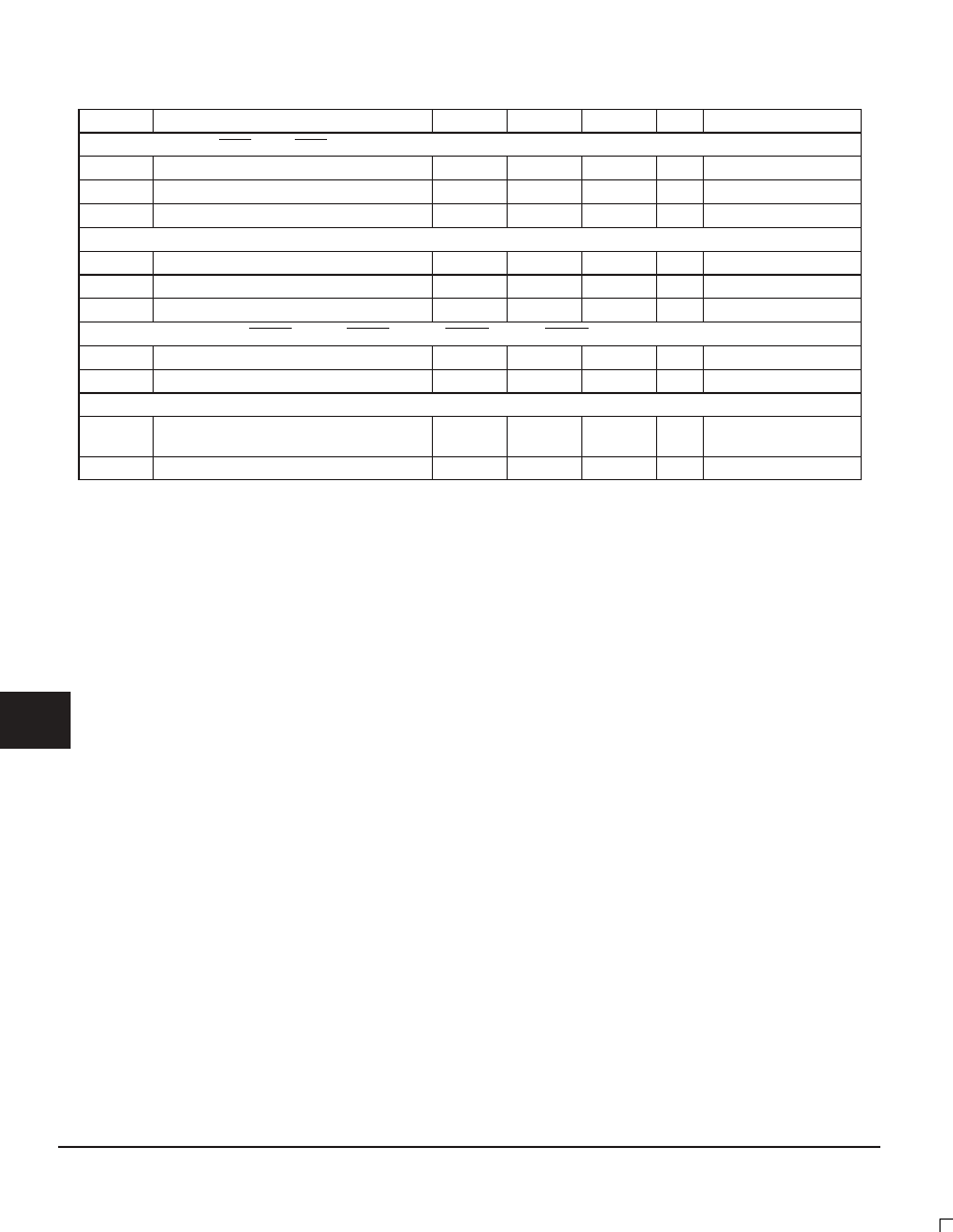
Table 6. ECL DC Characteristics (VEE = -2.5V ± 5% or VEE = -3.3V ± 5%, VCC = GND, TJ = TJ = 0°C to +110°C)
Symbol
Characteristics
Min
Typ
Max
Unit
Condition
Clock input pair CLK0, CLK0, CLK1, CLK1 (ECL differential signals)
VPP
Differential Input Voltagea
0.1
1.3
V
Differential operation
VCMR
Differential Cross Point Voltageb
VEE + 1.0
–0.3
V
Differential operation
IIN
Input Currenta
±150
A
VIN = VIL or VIN = VIH
Clock inputs MR, CLK_SEL, FSELA, FSELB, FSELC, FSELD (PECL single ended signals)
VIH
Input Voltage High
–1.165
-0.880
V
VIL
Input Voltage Low
–1.810
–1.475
V
IIN
Input Currentc
±150
A
VIN = VIL or VIN = VIH
ECL clock outputs (QA[0:1], QA[0:1], QB[0:2], QB[0:2], QC[0:3], QC[0:3], QD[0:5], QD[0:5]
VOH
Output High Voltage
–1.1
–1.005
–0.7
V
IOH = –30 mAd
VOL
Output Low Voltage
–1.9
–1.705
1.4
V
IOL = –5 mAd
Supply current and VBB
IEEe
Maximum Quiescent Supply Current without
output termination current
96
170
mA
VEE pins
VBB
Output reference voltage
-1.38
-1.22
V
IBB = 0.4 mA
a. VPP (DC) is the minimum differential input voltage swing required to maintain device functionality.
b. VCMR (DC) is the crosspoint of the differential input signal. Functional operation is obtained when the crosspoint is within the VCMR (DC)
range and the input swing lies within the VPP (DC) specification.
c. Input have internal pullup/pulldown resistors which affect the input current.
d. Equivalent to a termination of 50
W to VTT.
e. ICC calculation: ICC = (number of differential output used) x (IOH + IOL) + IEE
ICC = (number of differential output used) x (VOH – VTT )÷Rload + (VOL – V TT )÷Rload + IEE.
F
re
e
sc
a
le
S
e
m
ic
o
n
d
u
c
to
r,
I
Freescale Semiconductor, Inc.
For More Information On This Product,
Go to: www.freescale.com
n
c
..
.
相关PDF资料 |
PDF描述 |
|---|---|
| MC100ES6226AC | 100E SERIES, LOW SKEW CLOCK DRIVER, 9 TRUE OUTPUT(S), 0 INVERTED OUTPUT(S), PQFP32 |
| MC100ES7011HDR2 | 100E SERIES, LOW SKEW CLOCK DRIVER, 2 TRUE OUTPUT(S), 0 INVERTED OUTPUT(S), PDSO8 |
| MC100ES7011HD | 100E SERIES, LOW SKEW CLOCK DRIVER, 2 TRUE OUTPUT(S), 0 INVERTED OUTPUT(S), PDSO8 |
| MC100ES7011HDR2 | 100E SERIES, LOW SKEW CLOCK DRIVER, 2 TRUE OUTPUT(S), 0 INVERTED OUTPUT(S), PDSO8 |
| MC100ES7011PDR2 | 100E SERIES, LOW SKEW CLOCK DRIVER, 2 TRUE OUTPUT(S), 0 INVERTED OUTPUT(S), PDSO8 |
相关代理商/技术参数 |
参数描述 |
|---|---|
| MC100ES6226AC | 功能描述:时钟缓冲器 FSL 1-9 Diff LVPECL Clk Div Fanout Buff. RoHS:否 制造商:Texas Instruments 输出端数量:5 最大输入频率:40 MHz 传播延迟(最大值): 电源电压-最大:3.45 V 电源电压-最小:2.375 V 最大功率耗散: 最大工作温度:+ 85 C 最小工作温度:- 40 C 封装 / 箱体:LLP-24 封装:Reel |
| MC100ES6226ACR2 | 功能描述:时钟驱动器及分配 FSL 1-9 Diff LVPECL Clk Div Fanout Buff. RoHS:否 制造商:Micrel 乘法/除法因子:1:4 输出类型:Differential 最大输出频率:4.2 GHz 电源电压-最大: 电源电压-最小:5 V 最大工作温度:+ 85 C 封装 / 箱体:SOIC-8 封装:Reel |
| MC100ES6226FA | 功能描述:时钟缓冲器 Buffer RoHS:否 制造商:Texas Instruments 输出端数量:5 最大输入频率:40 MHz 传播延迟(最大值): 电源电压-最大:3.45 V 电源电压-最小:2.375 V 最大功率耗散: 最大工作温度:+ 85 C 最小工作温度:- 40 C 封装 / 箱体:LLP-24 封装:Reel |
| MC100ES6254AC | 功能描述:时钟驱动器及分配 FSL Differential LVP ECL 2x2 Clock Switch RoHS:否 制造商:Micrel 乘法/除法因子:1:4 输出类型:Differential 最大输出频率:4.2 GHz 电源电压-最大: 电源电压-最小:5 V 最大工作温度:+ 85 C 封装 / 箱体:SOIC-8 封装:Reel |
| MC100ES6254ACR2 | 功能描述:时钟驱动器及分配 FSL Differential LVP ECL 2x2 Clock Switch RoHS:否 制造商:Micrel 乘法/除法因子:1:4 输出类型:Differential 最大输出频率:4.2 GHz 电源电压-最大: 电源电压-最小:5 V 最大工作温度:+ 85 C 封装 / 箱体:SOIC-8 封装:Reel |
发布紧急采购,3分钟左右您将得到回复。