参数资料
| 型号: | MC26LS30DR2G |
| 厂商: | ON Semiconductor |
| 文件页数: | 9/14页 |
| 文件大小: | 0K |
| 描述: | IC DRIVER LINE CONFIG 16SOIC |
| 产品变化通告: | Product Obsolescence 24/Jan/2011 |
| 标准包装: | 1 |
| 类型: | 驱动器 |
| 驱动器/接收器数: | 4/0 |
| 规程: | RS422,RS423 |
| 电源电压: | 4.75 V ~ 5.25 V |
| 安装类型: | 表面贴装 |
| 封装/外壳: | 16-SOIC(0.154",3.90mm 宽) |
| 供应商设备封装: | 16-SOIC |
| 包装: | 剪切带 (CT) |
| 其它名称: | MC26LS30DR2GOSCT |
MC26LS30
http://onsemi.com
4
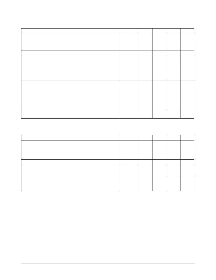
ELECTRICAL CHARACTERISTICS (EIA423A singleended mode, Pin 4
q 2.0 V, 40°C t TA t 85°C, 4.75 V p VCC,
Characteristic
Symbol
Min
Typ
Max
Unit
Output Voltage (VCC = VEE = 4.75 V)
VO1
VO2
4.0
3.6
4.2
3.95
0.05
6.0
0.4
Vdc
Slew Control Current (Pins 16, 13, 12, 9)
ISLEW
±120
A
Output Current (Each Output)
Power Off Leakage, VCC = VEE = 0, 6.0 V p VO p +6.0 V
Short Circuit Current (Output Short to Ground, Note 2)
Vin p 0.8 V (TA = 25°C)
Vin p 0.8 V (40°C t TA t +85°C)
Vin w 2.0 V (TA = 25°C)
Vin w 2.0 V (40°C t TA t +85°C)
IOLK
ISC+
ISC
100
60
50
150
0
80
95
+100
150
60
50
A
mA
Inputs
Low Level Voltage
High Level Voltage
Current @ Vin = 2.4 V
Current @ Vin = 15 V
Current @ Vin = 0.4 V
Current, 0
p Vin p 15 V, VCC = 0
Clamp Voltage (Iin = 12 mA)
VIL
VIH
IIH
IIHH
IIL
IIX
VIK
2.0
200
1.5
0
8.0
0
0.8
40
100
Vdc
A
Vdc
Power Supply Current (Outputs Open)
VCC = +5.25 V, VEE = 5.25 V, Vin = 0.4 V
ICC
IEE
22
17
8.0
30
mA
TIMING CHARACTERISTICS (EIA423A singleended mode, Pin 4
3) unless otherwise noted.)
Characteristic
Symbol
Min
Typ
Max
Unit
Output Timing (Figure 5)
Output Rise Time, CC = 0
Output Fall Time, CC = 0
Output Rise Time, CC = 50 pF
Output Fall Time, CC = 50 pF
tr
tf
tr
tf
65
3.0
300
ns
s
Rise Time Coefficient (Figure 16)
Crt
0.06
s/pF
Propagation Delay Time, Input to Single Ended Output (Figure 5)
Input Low to High, CC = 0
Input High to Low, CC = 0
tPDH
tPDL
100
300
ns
tPDH to tPDL for Each Driver
Max to Min tPDH Within a Package
Max to Min tPDL Within a Package
tSK4
tSK5
tSK6
15
2.0
5.0
ns
1. All voltages measured with respect to Pin 5.
2. Only one output shorted at a time, for not more than 1 second.
3. Typical values established at +25
°C, VCC = +5.0 V, VEE = 5.0 V.
4. Vin switched from 0.8 to 2.0 V.
5. Imbalance is the difference between
VO2 with Vin t 0.8 V and VO2 with Vin u 2.0 V.
相关PDF资料 |
PDF描述 |
|---|---|
| MC33388D | IC CAN FAULT TOL INTRFACE 14SOIC |
| MC33389DDW | IC SYSTEM BASE W/CAN 28-SOIC |
| MC33394DH | IC POWER SUPPLY MULT-OUT 44-HSOP |
| MC33560DW | OC PWR MGMT READERS/CPLR 24-SOIC |
| MC33689DDWBR2 | IC SYSTEM BASE W/LIN 32-SOIC |
相关代理商/技术参数 |
参数描述 |
|---|---|
| MC26LS31 | 制造商:MOTOROLA 制造商全称:Motorola, Inc 功能描述:Quad Line Driver with NAND Enabled Three-State Outputs |
| MC26LS31D | 制造商:Motorola Inc 功能描述: |
| MC26LS32D | 制造商:FREESCALE 制造商全称:Freescale Semiconductor, Inc 功能描述:QUAD EIA-422/3 LINE RECEIVER WITH THREE.STATE OUTPUTS |
| MC-27 | 制造商:Components Corporation 功能描述: |
| MC2707 | 制造商:M/A-COM Technology Solutions 功能描述:RF MIXER |
发布紧急采购,3分钟左右您将得到回复。