- 您现在的位置:买卖IC网 > PDF目录20420 > MC33152P (ON Semiconductor)IC DRIVER MOSFET DUAL HS 8DIP PDF资料下载
参数资料
| 型号: | MC33152P |
| 厂商: | ON Semiconductor |
| 文件页数: | 7/12页 |
| 文件大小: | 0K |
| 描述: | IC DRIVER MOSFET DUAL HS 8DIP |
| 产品变化通告: | LTB Notification 03/Jan/2008 |
| 标准包装: | 1,000 |
| 配置: | 低端 |
| 输入类型: | 非反相 |
| 延迟时间: | 55ns |
| 电流 - 峰: | 1.5A |
| 配置数: | 2 |
| 输出数: | 2 |
| 电源电压: | 6.1 V ~ 18 V |
| 工作温度: | -40°C ~ 85°C |
| 安装类型: | 通孔 |
| 封装/外壳: | 8-DIP(0.300",7.62mm) |
| 供应商设备封装: | 8-PDIP |
| 包装: | 管件 |
| 其它名称: | MC33152POS |
�� �
�
�MC34152,� MC33152,� NCV33152�
�the� NPN� pullup� during� the� negative� output� transient,� power�
�dissipation� at� high� frequencies� can� become� excessive.�
�Figures� 19,� 20,� and� 21� show� a� method� of� using� external�
�Schottky� diode� clamps� to� reduce� driver� power� dissipation.�
�Undervoltage� Lockout�
�An� undervoltage� lockout� with� hysteresis� prevents� erratic�
�system� operation� at� low� supply� voltages.� The� UVLO� forces�
�the� Drive� Outputs� into� a� low� state� as� V� CC� rises� from� 1.4� V�
�to� the� 5.8� V� upper� threshold.� The� lower� UVLO� threshold�
�is� 5.3� V,� yielding� about� 500� mV� of� hysteresis.�
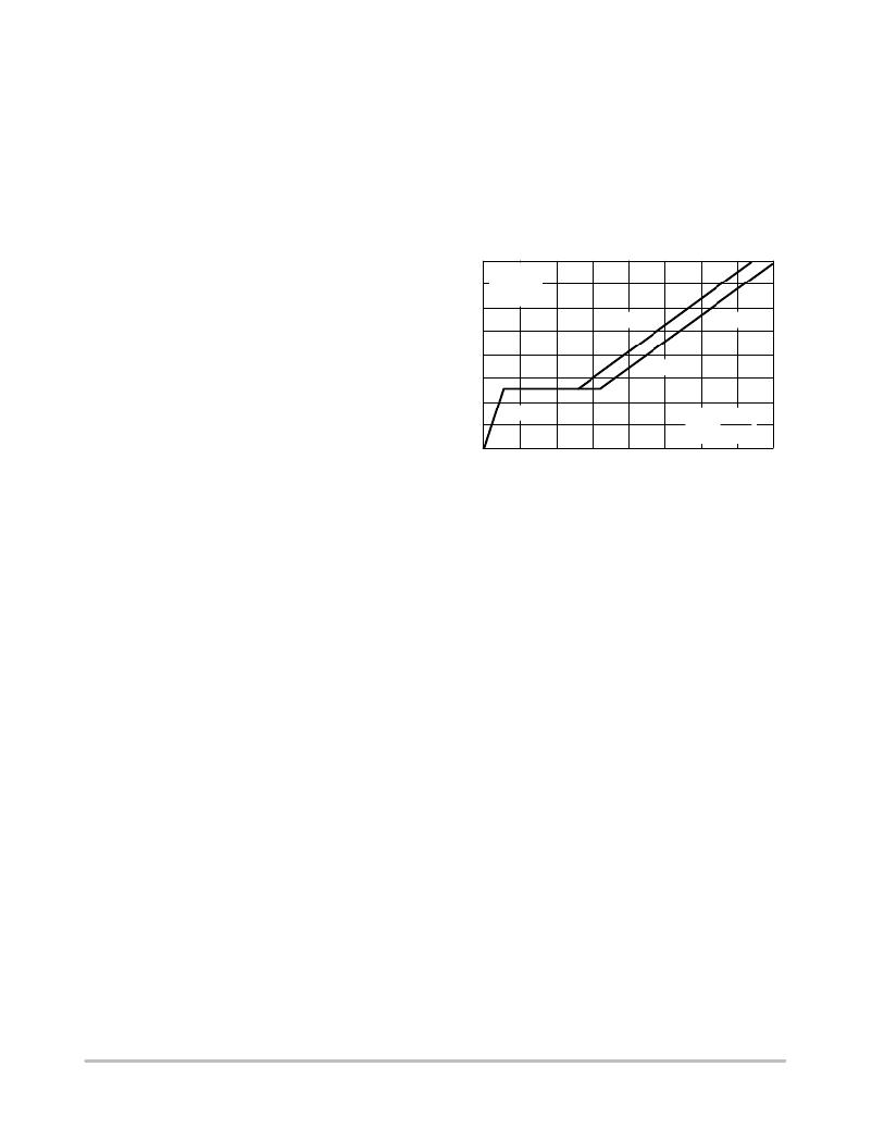
�aid� in� this� calculation,� power� MOSFET� manufacturers�
�provide� gate� charge� information� on� their� data� sheets.�
�Figure� 17� shows� a� curve� of� gate� voltage� versus� gate� charge�
�for� the� ON� Semiconductor� MTM15N50.� Note� that� there� are�
�three� distinct� slopes� to� the� curve� representing� different�
�input� capacitance� values.� To� completely� switch� the�
�MOSFET� ‘on,’� the� gate� must� be� brought� to� 10� V� with�
�respect� to� the� source.� The� graph� shows� that� a� gate� charge�
�Q� g� of� 110� nC� is� required� when� operating� the� MOSFET� with�
�a� drain� to� source� voltage� V� DS� of� 400� V.�
�Power� Dissipation�
�Circuit� performance� and� long� term� reliability� are�
�enhanced� with� reduced� die� temperature.� Die� temperature�
�increase� is� directly� related� to� the� power� that� the� integrated�
�16�
�12�
�MTM15B50�
�I� D� =� 15� A�
�T� A� =� 25� °� C�
�V� DS� =� 100� V�
�V� DS� =� 400� V�
�circuit� must� dissipate� and� the� total� thermal� resistance� from�
�the� junction� to� ambient.� The� formula� for� calculating� the�
�junction� temperature� with� the� package� in� free� air� is:�
�T� J� =� T� A� +� P� D� (R� q� JA� )�
�8.0�
�4.0�
�8.9 nF�
�where:�
�T� J� =� Junction� Temperature�
�T� A� =� Ambient� Temperature�
�P� D� =� Power� Dissipation�
�R� q� JA� =� Thermal� Resistance� Junction� to� Ambient�
�0�
�0�
�2.0� nF�
�40�
�D� Q� g�
�C� GS� =� D� V� GS�
�80� 120�
�Q� g� ,� GATE� CHARGE� (nC)�
�160�
�There� are� three� basic� components� that� make� up� total�
�power� to� be� dissipated� when� driving� a� capacitive� load� with�
�respect� to� ground.� They� are:�
�P� D� =� P� Q� +� P� C� +� P� T�
�where:� P� Q� =� Quiescent� Power� Dissipation�
�P� C� =� Capacitive� Load� Power� Dissipation�
�P� T� =� Transition� Power� Dissipation�
�The� quiescent� power� supply� current� depends� on� the�
�supply� voltage� and� duty� cycle� as� shown� in� Figure� 16.� The�
�device’s� quiescent� power� dissipation� is:�
�P� Q� =� V� CC� (I� CCL� [1� ?� D]� +� I� CCH� [D])�
�where:� I� CCL� =� Supply� Current� with� Low� State� Drive�
�Outputs�
�I� CCH� =� Supply� Current� with� High� State� Drive�
�Outputs�
�D� =� Output� Duty� Cycle�
�The� capacitive� load� power� dissipation� is� directly� related�
�to� the� load� capacitance� value,� frequency,� and� Drive� Output�
�voltage� swing.� The� capacitive� load� power� dissipation� per�
�driver� is:�
�P� C� =� V� CC� (V� OH� ?� V� OL� )� C� L� f�
�where:� V� OH� =� High� State� Drive� Output� Voltage�
�V� OL� =� Low� State� Drive� Output� Voltage�
�C� L� =� Load� Capacitance�
�f� =� Frequency�
�When� driving� a� MOSFET,� the� calculation� of� capacitive�
�load� power� P� C� is� somewhat� complicated� by� the� changing�
�gate� to� source� capacitance� C� GS� as� the� device� switches.� To�
�Figure� 17.� Gate� ?� to� ?� Source� Voltage�
�versus� Gate� charge�
�The� capacitive� load� power� dissipation� is� directly� related� to�
�the� required� gate� charge,� and� operating� frequency.� The�
�capacitive� load� power� dissipation� per� driver� is:�
�P� C(MOSFET)� =� V� CC� Q� g� f�
�The� flat� region� from� 10� nC� to� 55� nC� is� caused� by� the�
�drain� ?� to� ?� gate� Miller� capacitance,� occurring� while� the�
�MOSFET� is� in� the� linear� region� dissipating� substantial�
�amounts� of� power.� The� high� output� current� capability� of� the�
�MC34152� is� able� to� quickly� deliver� the� required� gate�
�charge� for� fast� power� efficient� MOSFET� switching.� By�
�operating� the� MC34152� at� a� higher� V� CC� ,� additional� charge�
�can� be� provided� to� bring� the� gate� above� 10� V.� This� will�
�reduce� the� ‘on’� resistance� of� the� MOSFET� at� the� expense�
�of� higher� driver� dissipation� at� a� given� operating� frequency.�
�The� transition� power� dissipation� is� due� to� extremely�
�short� simultaneous� conduction� of� internal� circuit� nodes�
�when� the� Drive� Outputs� change� state.� The� transition� power�
�dissipation� per� driver� is� approximately:�
�P� T� ≈� V� CC� (1.08� V� CC� C� L� f� ?� 8� x� 10� ?� 4� )�
�P� T� must� be� greater� than� zero.�
�Switching� time� characterization� of� the� MC34152� is�
�performed� with� fixed� capacitive� loads.� Figure� 13� shows�
�that� for� small� capacitance� loads,� the� switching� speed� is�
�limited� by� transistor� turn� ?� on/off� time� and� the� slew� rate� of�
�the� internal� nodes.� For� large� capacitance� loads,� the�
�switching� speed� is� limited� by� the� maximum� output� current�
�capability� of� the� integrated� circuit.�
�http://onsemi.com�
�7�
�相关PDF资料 |
PDF描述 |
|---|---|
| VI-BNM-CX-F3 | CONVERTER MOD DC/DC 10V 75W |
| 78F471J-RC | CHOKE CONFORMAL COATED 470UH |
| POE576U-24AFAT | POWER SUPPLY 24PORTS |
| SDR0604-180YL | INDUCTOR POWER 18UH 1.25A SMD |
| VE-J33-CW-F2 | CONVERTER MOD DC/DC 24V 100W |
相关代理商/技术参数 |
参数描述 |
|---|---|
| MC33152PG | 功能描述:功率驱动器IC 1.5A High Speed Dual Non-Inverting MOSFET RoHS:否 制造商:Micrel 产品:MOSFET Gate Drivers 类型:Low Cost High or Low Side MOSFET Driver 上升时间: 下降时间: 电源电压-最大:30 V 电源电压-最小:2.75 V 电源电流: 最大功率耗散: 最大工作温度:+ 85 C 安装风格:SMD/SMT 封装 / 箱体:SOIC-8 封装:Tube |
| MC33152VDG | 功能描述:功率驱动器IC ANA HI SPD DUAL DRIVER RoHS:否 制造商:Micrel 产品:MOSFET Gate Drivers 类型:Low Cost High or Low Side MOSFET Driver 上升时间: 下降时间: 电源电压-最大:30 V 电源电压-最小:2.75 V 电源电流: 最大功率耗散: 最大工作温度:+ 85 C 安装风格:SMD/SMT 封装 / 箱体:SOIC-8 封装:Tube |
| MC33152VDR2 | 功能描述:功率驱动器IC 1.5A High Speed Dual RoHS:否 制造商:Micrel 产品:MOSFET Gate Drivers 类型:Low Cost High or Low Side MOSFET Driver 上升时间: 下降时间: 电源电压-最大:30 V 电源电压-最小:2.75 V 电源电流: 最大功率耗散: 最大工作温度:+ 85 C 安装风格:SMD/SMT 封装 / 箱体:SOIC-8 封装:Tube |
| MC33152VDR2G | 功能描述:功率驱动器IC 1.5A High Speed Dual Non-Inverting MOSFET RoHS:否 制造商:Micrel 产品:MOSFET Gate Drivers 类型:Low Cost High or Low Side MOSFET Driver 上升时间: 下降时间: 电源电压-最大:30 V 电源电压-最小:2.75 V 电源电流: 最大功率耗散: 最大工作温度:+ 85 C 安装风格:SMD/SMT 封装 / 箱体:SOIC-8 封装:Tube |
| MC33153 | 制造商:SPC Multicomp 功能描述:FUSE RESETTABLE RADIAL 5A 制造商:SPC Multicomp 功能描述:FUSE, PTC RESET, RADIAL, 16V, 5A 制造商:SPC Multicomp 功能描述:FUSE, PTC RESET, 16V, 5A, RADIAL; Holding Current:5A; Tripping Current:8.5A; Initial Resistance Max:0.044ohm; Operating Voltage:16V; PTC Fuse Case:Radial Leaded; External Depth:3mm; Initial Resistance Min:0.014ohm; Lead Spacing:5.1mm;RoHS Compliant: Yes |
发布紧急采购,3分钟左右您将得到回复。