- 您现在的位置:买卖IC网 > PDF目录359133 > MC33989 (飞思卡尔半导体(中国)有限公司) System Basis Chip with High Speed CAN Transceiver(带高速CAN收发器的系统基片) PDF资料下载
参数资料
| 型号: | MC33989 |
| 厂商: | 飞思卡尔半导体(中国)有限公司 |
| 元件分类: | CAN |
| 英文描述: | System Basis Chip with High Speed CAN Transceiver(带高速CAN收发器的系统基片) |
| 中文描述: | 系统基础芯片的高速CAN收发器(带高速的CAN收发器的系统基片) |
| 文件页数: | 16/32页 |
| 文件大小: | 676K |
| 代理商: | MC33989 |
第1页第2页第3页第4页第5页第6页第7页第8页第9页第10页第11页第12页第13页第14页第15页当前第16页第17页第18页第19页第20页第21页第22页第23页第24页第25页第26页第27页第28页第29页第30页第31页第32页
16
MC33989
MC33989
and Tx pins are compatible to ISO11898 specification (IS0 11898: 1993(E)). The control of the CAN physical interface operation
is done through the SPI. CAN modes are independent of the SBC operation modes.
The device can wake up from a CAN message if CAN wake up has been enabled. Refer to CAN module description for detail
of wake up detection.
4.9.5
SPI wake up
The device can wake up by the CSB pin in sleep or stop mode. Wake up is detected by CSB pin transition from low to high
level. In stop mode this correspond to the condition where MCU and SBC are in Stop mode and when the application wake up
event comes through the MCU.
4.9.6
Device power up, SBC wake up
After device or system power up, or after the SBC wakes up from sleep mode, it enters into “reset mode” then into “normal
request mode”.
4.10
Debug mode: hardware and software debug with the SBC.
When the SBC is mounted on the same printed circuit board as the mico controller it supplies, both application software and
SBC dedicated routine must be debugged. Following features allow the user to debug the software by allowing the possibility to
disable the SBC internal software watchdog timer.
4.10.1
Device power up, reset pin connected to Vdd1
At SBC power up, the Vdd1 voltage is provided, but if no SPI communication occurs to configure the device, a reset occurs
every 350ms. In order to allow software debug and avoid MCU reset the Reset pin can be connected directly to Vdd1 by a jumper.
4.10.2
Debug modes with software watchdog disabled though SPI (Normal Debug, Standby Debug and Stop Debug)
The software watchdog can be disabled through SPI. In order to avoid unwanted watchdog disable and to limit the risk of
disabling the watchdog during SBC normal operation the watchdog disable has to be done with the following sequence:
Step 1) Power down the SBC
Step 2) Power up the SBC (The BATFAIL bit is set, and the SBC enters normal request mode)
Step 3) Write to TIM1 register to allow SBC to enter Normal mode
Step 4) Write to MCR register with data 0000 (this enables the debug mode). (Complete SPI byte: 000 1 0000)
Step 5) Write to MCR register normal debug (0001 x101)
While in debug mode, the SBC can be used without having to clear the W/D on a regular basis to facilitate software and
hardware debug.
Step 6) To leave the debug mode, write 0000 to MCR register.
At step 2, the SBC is in normal request. Step 3, 4 and 5 should be done consecutiveley and withing the 350ms time period of
the normal requets mode. If not, the SBC will go into reset mode and enter again normal request.
When the SBC is in debug mode, and has been set into stop debug or sleep debug, when a wake up occurs the SBC enters
Normal requets mode, for a time period of 350ms. In order to avoid the SBC to generate a reset (enter reset mode) the desired
next debug mode (normal debug or standby debug) should be configured within the 350ms time period of the normal requets
mode (for detail refer to “State machine in debug mode”).
To avoid entering debug mode after a power up, first read BATFAIL bit (MCR read) and write 0000 into MCR.
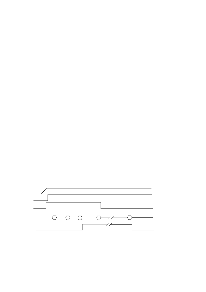
The graph below illustrates the debug mode enter.
4.10.3
MCU flash programming configuration
In order to allow the possibility to download software into the application memory (MCU EEPROM or Flash) the SBC allows
the following capabilities: The Vdd1 can be forced by an external power supply to 5V and the reset and Wdogb outputs by
external signal sources to zero or 5V and this without damage. This allow for instance to supply the complete application board by
external power supply and to apply the correct signal to reset pins.No function of the SBC are operating.
Due to pass transistor from Vdd1 to Vsup, supplying the device from Vdd1 pin biases the Vsup pin. So Vsup should be left
open of forced to value above 5V. Reset pin is periodically pulled low for “reset dur” time (3.4ms typical) and then pulled to Vdd1
for 350ms typical. During the time reset is low, reset pin sinks 5mA maximum (Ipdw parameter).
For More Information On This Product,
Go to: www.freescale.com
VSup
SPI
MCR(step4)
Batfail
Vdd1
debug mode
MCR (step5)
SPI: read batfail
MCR (step6)
SBC in debug Mode, no W/D
SBC not in debug Mode and W/D on
TIM1(step 3)
F
Freescale Semiconductor, Inc.
n
.
相关PDF资料 |
PDF描述 |
|---|---|
| MC33990 | J-1850 SERIAL TRANSCEIVER(J-1850总线收发器) |
| MC33991 | Gauge Driver Integrated Circuit(标尺驱动器集成电路) |
| MC33993 | Multiple Switch Detection Interface(多开关监测接口) |
| MC33997 | Switching Power Supply with Linear Regulators(带线性稳压器的开关电源) |
| MC33998 | Switching Power Supply with Linear Regulators(带线性稳压器的开关电源) |
相关代理商/技术参数 |
参数描述 |
|---|---|
| MC33989DW | 功能描述:CAN 接口集成电路 SBC HIGH SPEED RoHS:否 制造商:Texas Instruments 类型:Transceivers 工作电源电压:5 V 电源电流: 工作温度范围:- 40 C to + 85 C 封装 / 箱体:SOIC-8 封装:Tube |
| MC33989DWR2 | 功能描述:CAN 接口集成电路 SBC HIGH SPEED RoHS:否 制造商:Texas Instruments 类型:Transceivers 工作电源电压:5 V 电源电流: 工作温度范围:- 40 C to + 85 C 封装 / 箱体:SOIC-8 封装:Tube |
| MC33989PEG | 功能描述:CAN 接口集成电路 SBC-HS RoHS:否 制造商:Texas Instruments 类型:Transceivers 工作电源电压:5 V 电源电流: 工作温度范围:- 40 C to + 85 C 封装 / 箱体:SOIC-8 封装:Tube |
| MC33989PEGR2 | 功能描述:CAN 接口集成电路 SBC-HS RoHS:否 制造商:Texas Instruments 类型:Transceivers 工作电源电压:5 V 电源电流: 工作温度范围:- 40 C to + 85 C 封装 / 箱体:SOIC-8 封装:Tube |
| MC33990D | 功能描述:IC TRANSCEIVER J-1850 BUS 8-SOIC RoHS:否 类别:集成电路 (IC) >> 接口 - 驱动器,接收器,收发器 系列:- 标准包装:1,000 系列:- 类型:收发器 驱动器/接收器数:2/2 规程:RS232 电源电压:3 V ~ 5.5 V 安装类型:表面贴装 封装/外壳:16-SOIC(0.295",7.50mm 宽) 供应商设备封装:16-SOIC 包装:带卷 (TR) |
发布紧急采购,3分钟左右您将得到回复。