- 您现在的位置:买卖IC网 > PDF目录69024 > MC56F8006MLF (FREESCALE SEMICONDUCTOR INC) 16-BIT, FLASH, 32 MHz, MICROCONTROLLER, PQFP48 PDF资料下载
参数资料
| 型号: | MC56F8006MLF |
| 厂商: | FREESCALE SEMICONDUCTOR INC |
| 元件分类: | 微控制器/微处理器 |
| 英文描述: | 16-BIT, FLASH, 32 MHz, MICROCONTROLLER, PQFP48 |
| 封装: | 7 X 7 MM, 1.40 MM HEIGHT, 0.50 MM PITCH, ROHS COMPLIANT, MS-026BBC, LQFP-48 |
| 文件页数: | 39/106页 |
| 文件大小: | 1215K |
| 代理商: | MC56F8006MLF |
第1页第2页第3页第4页第5页第6页第7页第8页第9页第10页第11页第12页第13页第14页第15页第16页第17页第18页第19页第20页第21页第22页第23页第24页第25页第26页第27页第28页第29页第30页第31页第32页第33页第34页第35页第36页第37页第38页当前第39页第40页第41页第42页第43页第44页第45页第46页第47页第48页第49页第50页第51页第52页第53页第54页第55页第56页第57页第58页第59页第60页第61页第62页第63页第64页第65页第66页第67页第68页第69页第70页第71页第72页第73页第74页第75页第76页第77页第78页第79页第80页第81页第82页第83页第84页第85页第86页第87页第88页第89页第90页第91页第92页第93页第94页第95页第96页第97页第98页第99页第100页第101页第102页第103页第104页第105页第106页
MC56F8006/MC56F8002 Digital Signal Controller, Rev. 4
General System Control Information
Freescale Semiconductor
38
Registers containing the JTAG ID of the chip
Controls for programmable peripheral and GPIO connections
Peripheral clocks for TMR and PWM and SCI with a high-speed (3X) option
Power-saving clock gating for peripherals
Controls the enable/disable functions of large regulator standby mode with write protection capability
Permits selected peripherals to run in stop mode to generate stop recovery interrupts
Controls for programmable peripheral and GPIO connections
Software chip reset
I/O short address base location control
Peripheral protection control to provide runaway code protection for safety-critical applications
Controls output of internal clock sources to CLKO pin
Four general-purpose software control registers are reset only at power-on
Peripherals stop mode clocking control
6.7
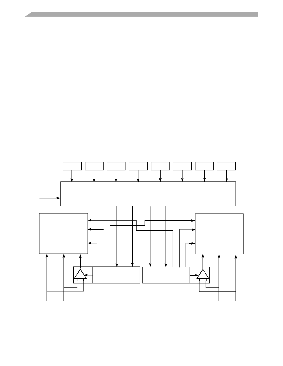
PWM, PDB, PGA, and ADC Connections
The comparators, timers, and PWM_reload_sync output can be connected to the programmable delay block (PDB) trigger input.
The PDB pre-trigger A and trigger A outputs are connected to the ADCA and PGA0 hardware trigger inputs. The PDB
pre-trigger B and trigger B outputs are connected to the ADCB and PGA1 hardware trigger inputs. When the input trigger of
PDB is asserted, PDB trigger and pre-trigger outputs are asserted after a delay of a pre-programmed period. See the MC56F8006
Peripheral Reference Manual for additional information.
Figure 15. Synchronization of ADC, PDB
TriggerA
Pre-
TriggerA
TriggerB
+
–
PGA0 Controller
ANA15
ANA9
ANA7
ADHWT
ADCA
Trigger
SSEL[0]
SSEL[1]
ADCA
+
–
PGA1 Controller
ANB15 ANB8
ANB6
ADHWT
ADCB
Trigger
SSEL[0]
SSEL[1]
ADCB
Pre-
TriggerB
System
Clock
TMR0
TMR1
SW
CMP0
CMP1
CMP2
PWM
EXT
Trigger0
Trigger1
Trigger2
Trigger3
Trigger4
Trigger5
Trigger6
Trigger7
Programmable Delay Block (PDB)
相关PDF资料 |
PDF描述 |
|---|---|
| MC56F8323MFB60 | 0-BIT, 120 MHz, OTHER DSP, PQFP64 |
| MC68020CFC25E | 32-BIT, 25 MHz, MICROPROCESSOR, PQFP132 |
| MC68020CFC25E | 32-BIT, 25 MHz, MICROPROCESSOR, PQFP132 |
| MC6804J1P | 8-BIT, MROM, MICROCONTROLLER, PDIP20 |
| MC6805S3VP | 8-BIT, MROM, 4.2 MHz, MICROCONTROLLER, PDIP28 |
相关代理商/技术参数 |
参数描述 |
|---|---|
| MC56F8006VBM | 功能描述:数字信号处理器和控制器 - DSP, DSC DSC 32SDIP 16K Flash RoHS:否 制造商:Microchip Technology 核心:dsPIC 数据总线宽度:16 bit 程序存储器大小:16 KB 数据 RAM 大小:2 KB 最大时钟频率:40 MHz 可编程输入/输出端数量:35 定时器数量:3 设备每秒兆指令数:50 MIPs 工作电源电压:3.3 V 最大工作温度:+ 85 C 封装 / 箱体:TQFP-44 安装风格:SMD/SMT |
| MC56F8006VLC | 功能描述:数字信号处理器和控制器 - DSP, DSC DSC 32LQFP 16K Flash RoHS:否 制造商:Microchip Technology 核心:dsPIC 数据总线宽度:16 bit 程序存储器大小:16 KB 数据 RAM 大小:2 KB 最大时钟频率:40 MHz 可编程输入/输出端数量:35 定时器数量:3 设备每秒兆指令数:50 MIPs 工作电源电压:3.3 V 最大工作温度:+ 85 C 封装 / 箱体:TQFP-44 安装风格:SMD/SMT |
| MC56F8006VLF | 功能描述:数字信号处理器和控制器 - DSP, DSC DSC 48LQFP 16K Flash RoHS:否 制造商:Microchip Technology 核心:dsPIC 数据总线宽度:16 bit 程序存储器大小:16 KB 数据 RAM 大小:2 KB 最大时钟频率:40 MHz 可编程输入/输出端数量:35 定时器数量:3 设备每秒兆指令数:50 MIPs 工作电源电压:3.3 V 最大工作温度:+ 85 C 封装 / 箱体:TQFP-44 安装风格:SMD/SMT |
| MC56F8006VLF | 制造商:Freescale Semiconductor 功能描述:IC DSC 16BIT 16KB 32MHZ 3.6V LQFP-48 |
| MC56F8006VWL | 功能描述:数字信号处理器和控制器 - DSP, DSC 16 BIT DSPHC RoHS:否 制造商:Microchip Technology 核心:dsPIC 数据总线宽度:16 bit 程序存储器大小:16 KB 数据 RAM 大小:2 KB 最大时钟频率:40 MHz 可编程输入/输出端数量:35 定时器数量:3 设备每秒兆指令数:50 MIPs 工作电源电压:3.3 V 最大工作温度:+ 85 C 封装 / 箱体:TQFP-44 安装风格:SMD/SMT |
发布紧急采购,3分钟左右您将得到回复。