- 您现在的位置:买卖IC网 > PDF目录45206 > MC56F8145VFG (FREESCALE SEMICONDUCTOR INC) 4-BIT, 120 MHz, OTHER DSP, PQFP128 PDF资料下载
参数资料
| 型号: | MC56F8145VFG |
| 厂商: | FREESCALE SEMICONDUCTOR INC |
| 元件分类: | 数字信号处理 |
| 英文描述: | 4-BIT, 120 MHz, OTHER DSP, PQFP128 |
| 封装: | PLASTIC, LQFP-128 |
| 文件页数: | 16/172页 |
| 文件大小: | 871K |
| 代理商: | MC56F8145VFG |
第1页第2页第3页第4页第5页第6页第7页第8页第9页第10页第11页第12页第13页第14页第15页当前第16页第17页第18页第19页第20页第21页第22页第23页第24页第25页第26页第27页第28页第29页第30页第31页第32页第33页第34页第35页第36页第37页第38页第39页第40页第41页第42页第43页第44页第45页第46页第47页第48页第49页第50页第51页第52页第53页第54页第55页第56页第57页第58页第59页第60页第61页第62页第63页第64页第65页第66页第67页第68页第69页第70页第71页第72页第73页第74页第75页第76页第77页第78页第79页第80页第81页第82页第83页第84页第85页第86页第87页第88页第89页第90页第91页第92页第93页第94页第95页第96页第97页第98页第99页第100页第101页第102页第103页第104页第105页第106页第107页第108页第109页第110页第111页第112页第113页第114页第115页第116页第117页第118页第119页第120页第121页第122页第123页第124页第125页第126页第127页第128页第129页第130页第131页第132页第133页第134页第135页第136页第137页第138页第139页第140页第141页第142页第143页第144页第145页第146页第147页第148页第149页第150页第151页第152页第153页第154页第155页第156页第157页第158页第159页第160页第161页第162页第163页第164页第165页第166页第167页第168页第169页第170页第171页第172页
56F8345 Technical Data, Rev. 17
112
Freescale Semiconductor
Preliminary
6.5.6.14
Reserved—Bit 2–0
This bit field is reserved or not implemented. It is read as 0 and cannot be modified by writing.
6.5.7
CLKO Select Register (SIM_CLKOSR)
The CLKO select register can be used to multiplex out any one of the clocks generated inside the clock
generation and SIM modules. The default value is SYS_CLK. This path has been optimized in order to
minimize any delay and clock duty cycle distortion. All other clocks primarily muxed out are for test
purposes only, and are subject to significant phase shift at high frequencies.
The upper four bits of the GPIOB register can function as GPIO, [A23:A20], or as additional clock output
signals. GPIO has priority and is enabled/disabled via the GPIOB_PER. If GPIOB[7:4] are programmed
to operate as peripheral outputs, then the choice between [A23:A20] and additional clock outputs is done
here in the CLKOSR. The default state is for the peripheral function of GPIOB[7:4] to be programmed as
[A23:A20]. This can be changed by altering [A23:A20], as shown in Figure 6-9.
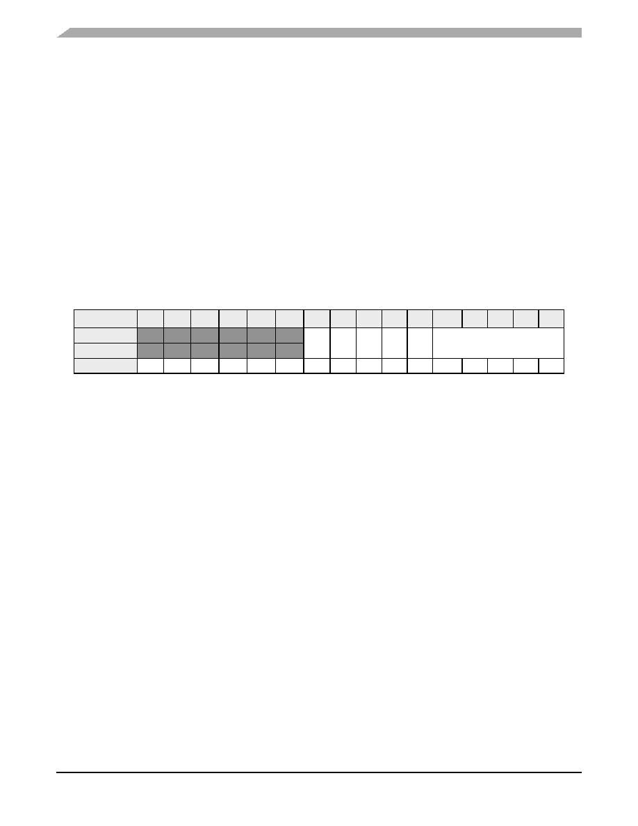
Figure 6-9 CLKO Select Register (SIM_CLKOSR)
6.5.7.1
Reserved—Bits 15–10
This bit field is reserved or not implemented. It is read as 0 and cannot be modified by writing.
6.5.7.2
Alternate GPIO_B Peripheral Function for A23 (A23)—Bit 9
0 = Peripheral output function of GPIOB[7] is defined to be A[23]
1 = Peripheral output function of GPIOB[7] is defined to be the oscillator clock (MSTR_OSC, see
6.5.7.3
Alternate GPIO_B Peripheral Function for A22 (A22)—Bit 8
0 = Peripheral output function of GPIOB[6] is defined to be A[22]
1 = Peripheral output function of GPIOB[6] is defined to be SYS_CLK2
6.5.7.4
Alternate GPIO_B Peripheral Function for A21 (A21)—Bit 7
0 = Peripheral output function of GPIOB[5] is defined to be A[21]
1 = Peripheral output function of GPIOB[5] is defined to be SYS_CLK
6.5.7.5
Alternate GPIO_B Peripheral Function for A20 (A20)—Bit 6
0 = Peripheral output function of GPIOB[4] is defined to be A[20]
1 = Peripheral output function of GPIOB[4] is defined to be the prescaler clock (FREF, see Figure 3-4)
Base + $A
15
14
13
12
11
10
9
8
7
6
5
4
3
2
1
0
Read
0
A23
A22
A21
A20
CLK
DIS
CLKOSEL
Write
RESET
0
001
0
000
0
相关PDF资料 |
PDF描述 |
|---|---|
| MC56F8146VFVE | 16-BIT, 120 MHz, OTHER DSP, PQFP144 |
| MC56F8146VFV | 16-BIT, 120 MHz, OTHER DSP, PQFP144 |
| MC56F8167VPYE | 16-BIT, 120 MHz, OTHER DSP, PQFP160 |
| MC56F8367VVFE | 16-BIT, 120 MHz, OTHER DSP, PBGA160 |
| MC56F8367VVF | 16-BIT, 120 MHz, OTHER DSP, PBGA160 |
相关代理商/技术参数 |
参数描述 |
|---|---|
| MC56F8145VFGE | 功能描述:数字信号处理器和控制器 - DSP, DSC 16 BIT HYBRID CONTROLLER RoHS:否 制造商:Microchip Technology 核心:dsPIC 数据总线宽度:16 bit 程序存储器大小:16 KB 数据 RAM 大小:2 KB 最大时钟频率:40 MHz 可编程输入/输出端数量:35 定时器数量:3 设备每秒兆指令数:50 MIPs 工作电源电压:3.3 V 最大工作温度:+ 85 C 封装 / 箱体:TQFP-44 安装风格:SMD/SMT |
| MC56F8145VFGER | 功能描述:数字信号处理器和控制器 - DSP, DSC 16 BIT HYBRID CONTROLLER RoHS:否 制造商:Microchip Technology 核心:dsPIC 数据总线宽度:16 bit 程序存储器大小:16 KB 数据 RAM 大小:2 KB 最大时钟频率:40 MHz 可编程输入/输出端数量:35 定时器数量:3 设备每秒兆指令数:50 MIPs 工作电源电压:3.3 V 最大工作温度:+ 85 C 封装 / 箱体:TQFP-44 安装风格:SMD/SMT |
| MC56F8146 | 制造商:FREESCALE 制造商全称:Freescale Semiconductor, Inc 功能描述:16-bit Digital Signal Controllers |
| MC56F8146VFV | 制造商:Rochester Electronics LLC 功能描述:- Bulk |
| MC56F8146VFVE | 功能描述:数字信号处理器和控制器 - DSP, DSC 16 BIT HYBRID CONTROLLER RoHS:否 制造商:Microchip Technology 核心:dsPIC 数据总线宽度:16 bit 程序存储器大小:16 KB 数据 RAM 大小:2 KB 最大时钟频率:40 MHz 可编程输入/输出端数量:35 定时器数量:3 设备每秒兆指令数:50 MIPs 工作电源电压:3.3 V 最大工作温度:+ 85 C 封装 / 箱体:TQFP-44 安装风格:SMD/SMT |
发布紧急采购,3分钟左右您将得到回复。