- 您现在的位置:买卖IC网 > PDF目录11942 > MC68711D3CFBE2 (Freescale Semiconductor)IC MCU 8BIT 44-QFP PDF资料下载
参数资料
| 型号: | MC68711D3CFBE2 |
| 厂商: | Freescale Semiconductor |
| 文件页数: | 113/124页 |
| 文件大小: | 0K |
| 描述: | IC MCU 8BIT 44-QFP |
| 标准包装: | 96 |
| 系列: | HC11 |
| 核心处理器: | HC11 |
| 芯体尺寸: | 8-位 |
| 速度: | 2MHz |
| 连通性: | SCI,SPI |
| 外围设备: | POR,WDT |
| 输入/输出数: | 26 |
| 程序存储器容量: | 4KB(4K x 8) |
| 程序存储器类型: | OTP |
| RAM 容量: | 192 x 8 |
| 电压 - 电源 (Vcc/Vdd): | 4.5 V ~ 5.5 V |
| 振荡器型: | 内部 |
| 工作温度: | -40°C ~ 85°C |
| 封装/外壳: | 44-QFP |
| 包装: | 托盘 |
第1页第2页第3页第4页第5页第6页第7页第8页第9页第10页第11页第12页第13页第14页第15页第16页第17页第18页第19页第20页第21页第22页第23页第24页第25页第26页第27页第28页第29页第30页第31页第32页第33页第34页第35页第36页第37页第38页第39页第40页第41页第42页第43页第44页第45页第46页第47页第48页第49页第50页第51页第52页第53页第54页第55页第56页第57页第58页第59页第60页第61页第62页第63页第64页第65页第66页第67页第68页第69页第70页第71页第72页第73页第74页第75页第76页第77页第78页第79页第80页第81页第82页第83页第84页第85页第86页第87页第88页第89页第90页第91页第92页第93页第94页第95页第96页第97页第98页第99页第100页第101页第102页第103页第104页第105页第106页第107页第108页第109页第110页第111页第112页当前第113页第114页第115页第116页第117页第118页第119页第120页第121页第122页第123页第124页
TIMING SYSTEM
TECHNICAL DATA
9-3
9.1 Timer Structure
Figure 9-1 shows the capture/compare system block diagram. The port A pin control
block includes logic for timer functions and for general-purpose I/O. For pins PA2,
PA1, and PA0, this block contains both the edge-detection logic and the control logic
that enables the selection of which edge triggers an input capture. The digital level on
PA[2:0] can be read at any time (read PORTA register), even if the pin is being used
for the input capture function. Pins PA[6:4] are used for either general-purpose output,
or as output compare pins. Pin PA3 can be used for general-purpose I/O, input capture
4, output compare 5, or output compare 1. When one of these pins is being used for
an output compare function, it cannot be written directly as if it were a general-purpose
output. Each of the output compare functions (OC5–OC2) is related to one of the port
A output pins. Output compare one (OC1) has extra control logic, allowing it optional
control of any combination of the PA[7:3] pins. The PA7 pin can be used as a general-
purpose I/O pin, as an input to the pulse accumulator, or as an OC1 output pin.
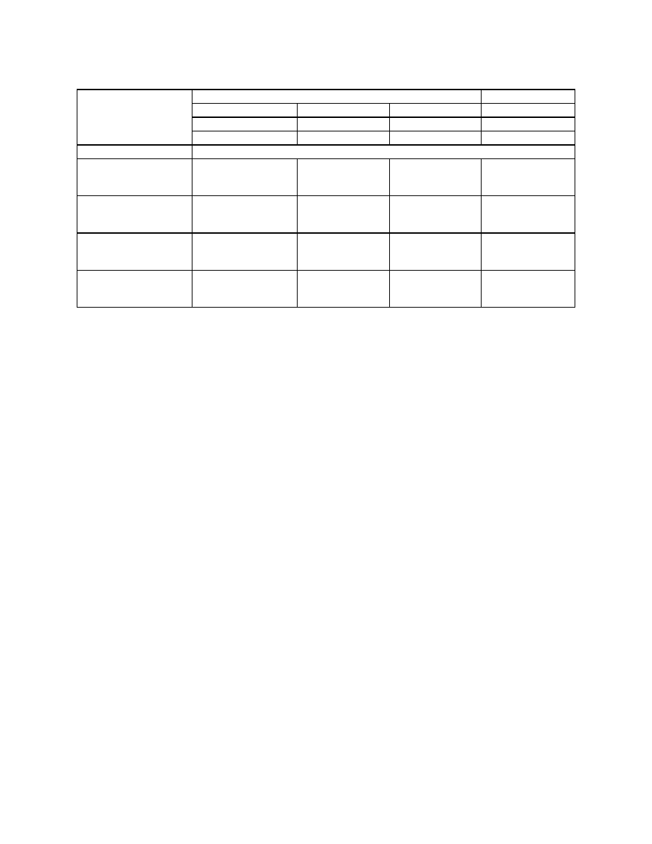
Table 9-1 Timer Summary
XTAL Frequencies
4.0 MHz
8.0 MHz
12.0 MHz
Other Rates
Control
1.0 MHz
2.0 MHz
3.0 MHz
(E)
Bits
1000 ns
500 ns
333 ns
(1/E)
PR[1:0]
Main Timer Count Rates
0 0
1 count —
overflow —
1.0 s
65.536 ms
500 ns
32.768 ms
333 ns
21.845 ms
(E/1)
(E/216)
0 1
1 count —
overflow —
4.0 s
262.14 ms
2.0 s
131.07 ms
1.333 s
87.381 ms
(E/4)
(E/218)
1 0
1 count —
overflow —
8.0 s
524.29 ms
4.0 s
262.14 ms
2.667 s
174.76 ms
(E/8)
(E/219)
1 1
1 count —
overflow —
16.0 s
1.049 s
8.0 s
524.29 ms
5.333 s
349.52 ms
(E/16)
(E/220)
F
re
e
sc
a
le
S
e
m
ic
o
n
d
u
c
to
r,
I
Freescale Semiconductor, Inc.
For More Information On This Product,
Go to: www.freescale.com
n
c
..
.
相关PDF资料 |
PDF描述 |
|---|---|
| VE-B11-CU-F4 | CONVERTER MOD DC/DC 12V 200W |
| MC68711E20CFNE3 | IC MCU 8BIT 52-PLCC |
| HCE103MBCDJ0KR | CAP CER 10000PF 3KV 20% RADIAL |
| MC68711E20CFUE2 | IC MCU 8BIT 64-QFP |
| HCE103MBCDF0KR | CAP CER 10000PF 3KV 20% RADIAL |
相关代理商/技术参数 |
参数描述 |
|---|---|
| MC68711E20CFNE2 | 功能描述:8位微控制器 -MCU 8B 20K EPROM 768RAM RoHS:否 制造商:Silicon Labs 核心:8051 处理器系列:C8051F39x 数据总线宽度:8 bit 最大时钟频率:50 MHz 程序存储器大小:16 KB 数据 RAM 大小:1 KB 片上 ADC:Yes 工作电源电压:1.8 V to 3.6 V 工作温度范围:- 40 C to + 105 C 封装 / 箱体:QFN-20 安装风格:SMD/SMT |
| MC68711E20CFNE2 | 制造商:Freescale Semiconductor 功能描述:8-Bit Microcontroller IC |
| MC68711E20CFNE3 | 功能描述:8位微控制器 -MCU 8B 20K EPROM 768RAM RoHS:否 制造商:Silicon Labs 核心:8051 处理器系列:C8051F39x 数据总线宽度:8 bit 最大时钟频率:50 MHz 程序存储器大小:16 KB 数据 RAM 大小:1 KB 片上 ADC:Yes 工作电源电压:1.8 V to 3.6 V 工作温度范围:- 40 C to + 105 C 封装 / 箱体:QFN-20 安装风格:SMD/SMT |
| MC68711E20CFNE4 | 功能描述:8位微控制器 -MCU 8B 20K EPROM 768RAM RoHS:否 制造商:Silicon Labs 核心:8051 处理器系列:C8051F39x 数据总线宽度:8 bit 最大时钟频率:50 MHz 程序存储器大小:16 KB 数据 RAM 大小:1 KB 片上 ADC:Yes 工作电源电压:1.8 V to 3.6 V 工作温度范围:- 40 C to + 105 C 封装 / 箱体:QFN-20 安装风格:SMD/SMT |
| MC68711E20CFUE2 | 功能描述:IC MCU 8BIT 64-QFP RoHS:是 类别:集成电路 (IC) >> 嵌入式 - 微控制器, 系列:HC11 标准包装:1 系列:AVR® ATmega 核心处理器:AVR 芯体尺寸:8-位 速度:16MHz 连通性:I²C,SPI,UART/USART 外围设备:欠压检测/复位,POR,PWM,WDT 输入/输出数:32 程序存储器容量:32KB(16K x 16) 程序存储器类型:闪存 EEPROM 大小:1K x 8 RAM 容量:2K x 8 电压 - 电源 (Vcc/Vdd):2.7 V ~ 5.5 V 数据转换器:A/D 8x10b 振荡器型:内部 工作温度:-40°C ~ 125°C 封装/外壳:44-TQFP 包装:剪切带 (CT) 其它名称:ATMEGA324P-B15AZCT |
发布紧急采购,3分钟左右您将得到回复。