- 您现在的位置:买卖IC网 > PDF目录11942 > MC68711D3CFBE2 (Freescale Semiconductor)IC MCU 8BIT 44-QFP PDF资料下载
参数资料
| 型号: | MC68711D3CFBE2 |
| 厂商: | Freescale Semiconductor |
| 文件页数: | 86/124页 |
| 文件大小: | 0K |
| 描述: | IC MCU 8BIT 44-QFP |
| 标准包装: | 96 |
| 系列: | HC11 |
| 核心处理器: | HC11 |
| 芯体尺寸: | 8-位 |
| 速度: | 2MHz |
| 连通性: | SCI,SPI |
| 外围设备: | POR,WDT |
| 输入/输出数: | 26 |
| 程序存储器容量: | 4KB(4K x 8) |
| 程序存储器类型: | OTP |
| RAM 容量: | 192 x 8 |
| 电压 - 电源 (Vcc/Vdd): | 4.5 V ~ 5.5 V |
| 振荡器型: | 内部 |
| 工作温度: | -40°C ~ 85°C |
| 封装/外壳: | 44-QFP |
| 包装: | 托盘 |
第1页第2页第3页第4页第5页第6页第7页第8页第9页第10页第11页第12页第13页第14页第15页第16页第17页第18页第19页第20页第21页第22页第23页第24页第25页第26页第27页第28页第29页第30页第31页第32页第33页第34页第35页第36页第37页第38页第39页第40页第41页第42页第43页第44页第45页第46页第47页第48页第49页第50页第51页第52页第53页第54页第55页第56页第57页第58页第59页第60页第61页第62页第63页第64页第65页第66页第67页第68页第69页第70页第71页第72页第73页第74页第75页第76页第77页第78页第79页第80页第81页第82页第83页第84页第85页当前第86页第87页第88页第89页第90页第91页第92页第93页第94页第95页第96页第97页第98页第99页第100页第101页第102页第103页第104页第105页第106页第107页第108页第109页第110页第111页第112页第113页第114页第115页第116页第117页第118页第119页第120页第121页第122页第123页第124页
PARALLEL I/O
6-2
TECHNICAL DATA
DDB[7:0] — Data Direction for Port B
0 = Corresponding port B pin configured for input only
1 = Corresponding port B pin configured as output
6.3 Port C
Port C pins are general-purpose I/O (PC[7:0]) in single-chip mode. In expanded mul-
tiplexed mode, port C pins are configured as multiplexed address/data pins. During the
data cycle, bits [7:0] (PC[7:0]) are bidirectional data pins controlled by the R/W signal.
DDC[7:0] — Data Direction for Port C
0 = Input
1 = Output
6.4 Port D
The eight port D bits (PD[7:0]) can be used for general-purpose I/O, for the SCI and
SPI subsystems, or for bus data direction control. Port D can be read at any time. In-
puts return the sensed levels at the pin; outputs return the input level of the port D pin
drivers. If port D is written, the data is stored in an internal latch, and can be driven only
if port D is configured for general-purpose output. This port shares functions with the
on-chip SCI and SPI subsystems, while bits 6 and 7 control the direction of data flow
on the bus in expanded and special test modes.
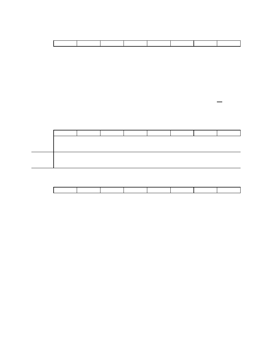
DDRB — Data Direction Register for Port B
$0006
Bit 7
654321
Bit 0
DDB7
DDB6
DDB5
DDC4
DDB3
DDB2
DDB1
DDB0
RESET:
00000000
PORTC — Port C Data
$0003
Bit 7
654321
Bit 0
PC7
PC6
PC5
PC4
PC3
PC2
PC1
PC0
S. Chip
or Boot:
PC7
PC6
PC5
PC4
PC3
PC2
PC1
PC0
RESET:
Reset configures pins as HiZ inputs
Expan.
or Test:
ADDR7/
DATA7
ADDR6/
DATA6
ADDR5/
DATA5
ADDR4/
DATA4
ADDR3/
DATA3
ADDR2/
DATA2
ADDR1/
DATA1
ADDR0/
DATA0
RESET:
Reset configures pins as multiplexed, low-order address/data I/O
DDRC — Data Direction Register for Port C
$0007
Bit 7
654321
Bit 0
DDC7
DDC6
DDC5
DDC4
DDC3
DDC2
DDC1
DDC0
RESET:
00000000
F
re
e
sc
a
le
S
e
m
ic
o
n
d
u
c
to
r,
I
Freescale Semiconductor, Inc.
For More Information On This Product,
Go to: www.freescale.com
n
c
..
.
相关PDF资料 |
PDF描述 |
|---|---|
| VE-B11-CU-F4 | CONVERTER MOD DC/DC 12V 200W |
| MC68711E20CFNE3 | IC MCU 8BIT 52-PLCC |
| HCE103MBCDJ0KR | CAP CER 10000PF 3KV 20% RADIAL |
| MC68711E20CFUE2 | IC MCU 8BIT 64-QFP |
| HCE103MBCDF0KR | CAP CER 10000PF 3KV 20% RADIAL |
相关代理商/技术参数 |
参数描述 |
|---|---|
| MC68711E20CFNE2 | 功能描述:8位微控制器 -MCU 8B 20K EPROM 768RAM RoHS:否 制造商:Silicon Labs 核心:8051 处理器系列:C8051F39x 数据总线宽度:8 bit 最大时钟频率:50 MHz 程序存储器大小:16 KB 数据 RAM 大小:1 KB 片上 ADC:Yes 工作电源电压:1.8 V to 3.6 V 工作温度范围:- 40 C to + 105 C 封装 / 箱体:QFN-20 安装风格:SMD/SMT |
| MC68711E20CFNE2 | 制造商:Freescale Semiconductor 功能描述:8-Bit Microcontroller IC |
| MC68711E20CFNE3 | 功能描述:8位微控制器 -MCU 8B 20K EPROM 768RAM RoHS:否 制造商:Silicon Labs 核心:8051 处理器系列:C8051F39x 数据总线宽度:8 bit 最大时钟频率:50 MHz 程序存储器大小:16 KB 数据 RAM 大小:1 KB 片上 ADC:Yes 工作电源电压:1.8 V to 3.6 V 工作温度范围:- 40 C to + 105 C 封装 / 箱体:QFN-20 安装风格:SMD/SMT |
| MC68711E20CFNE4 | 功能描述:8位微控制器 -MCU 8B 20K EPROM 768RAM RoHS:否 制造商:Silicon Labs 核心:8051 处理器系列:C8051F39x 数据总线宽度:8 bit 最大时钟频率:50 MHz 程序存储器大小:16 KB 数据 RAM 大小:1 KB 片上 ADC:Yes 工作电源电压:1.8 V to 3.6 V 工作温度范围:- 40 C to + 105 C 封装 / 箱体:QFN-20 安装风格:SMD/SMT |
| MC68711E20CFUE2 | 功能描述:IC MCU 8BIT 64-QFP RoHS:是 类别:集成电路 (IC) >> 嵌入式 - 微控制器, 系列:HC11 标准包装:1 系列:AVR® ATmega 核心处理器:AVR 芯体尺寸:8-位 速度:16MHz 连通性:I²C,SPI,UART/USART 外围设备:欠压检测/复位,POR,PWM,WDT 输入/输出数:32 程序存储器容量:32KB(16K x 16) 程序存储器类型:闪存 EEPROM 大小:1K x 8 RAM 容量:2K x 8 电压 - 电源 (Vcc/Vdd):2.7 V ~ 5.5 V 数据转换器:A/D 8x10b 振荡器型:内部 工作温度:-40°C ~ 125°C 封装/外壳:44-TQFP 包装:剪切带 (CT) 其它名称:ATMEGA324P-B15AZCT |
发布紧急采购,3分钟左右您将得到回复。