- 您现在的位置:买卖IC网 > PDF目录201871 > MC68HC08AS32ACFU (FREESCALE SEMICONDUCTOR INC) 8-BIT, MROM, 8.4 MHz, MICROCONTROLLER, PQFP64 PDF资料下载
参数资料
| 型号: | MC68HC08AS32ACFU |
| 厂商: | FREESCALE SEMICONDUCTOR INC |
| 元件分类: | 微控制器/微处理器 |
| 英文描述: | 8-BIT, MROM, 8.4 MHz, MICROCONTROLLER, PQFP64 |
| 封装: | QFP-64 |
| 文件页数: | 296/296页 |
| 文件大小: | 3608K |
| 代理商: | MC68HC08AS32ACFU |
第1页第2页第3页第4页第5页第6页第7页第8页第9页第10页第11页第12页第13页第14页第15页第16页第17页第18页第19页第20页第21页第22页第23页第24页第25页第26页第27页第28页第29页第30页第31页第32页第33页第34页第35页第36页第37页第38页第39页第40页第41页第42页第43页第44页第45页第46页第47页第48页第49页第50页第51页第52页第53页第54页第55页第56页第57页第58页第59页第60页第61页第62页第63页第64页第65页第66页第67页第68页第69页第70页第71页第72页第73页第74页第75页第76页第77页第78页第79页第80页第81页第82页第83页第84页第85页第86页第87页第88页第89页第90页第91页第92页第93页第94页第95页第96页第97页第98页第99页第100页第101页第102页第103页第104页第105页第106页第107页第108页第109页第110页第111页第112页第113页第114页第115页第116页第117页第118页第119页第120页第121页第122页第123页第124页第125页第126页第127页第128页第129页第130页第131页第132页第133页第134页第135页第136页第137页第138页第139页第140页第141页第142页第143页第144页第145页第146页第147页第148页第149页第150页第151页第152页第153页第154页第155页第156页第157页第158页第159页第160页第161页第162页第163页第164页第165页第166页第167页第168页第169页第170页第171页第172页第173页第174页第175页第176页第177页第178页第179页第180页第181页第182页第183页第184页第185页第186页第187页第188页第189页第190页第191页第192页第193页第194页第195页第196页第197页第198页第199页第200页第201页第202页第203页第204页第205页第206页第207页第208页第209页第210页第211页第212页第213页第214页第215页第216页第217页第218页第219页第220页第221页第222页第223页第224页第225页第226页第227页第228页第229页第230页第231页第232页第233页第234页第235页第236页第237页第238页第239页第240页第241页第242页第243页第244页第245页第246页第247页第248页第249页第250页第251页第252页第253页第254页第255页第256页第257页第258页第259页第260页第261页第262页第263页第264页第265页第266页第267页第268页第269页第270页第271页第272页第273页第274页第275页第276页第277页第278页第279页第280页第281页第282页第283页第284页第285页第286页第287页第288页第289页第290页第291页第292页第293页第294页第295页当前第296页
MC68HC08AS32A — Rev. 1.1
Data Sheet
Freescale Semiconductor
99
5.3.1 Crystal Oscillator Circuit
The crystal oscillator circuit consists of an inverting amplifier and an external
crystal. The OSC1 pin is the input and the OSC2 pin is the output to the amplifier.
The SIMOSCEN signal from the system integration module (SIM) enables the
crystal oscillator circuit.
The CGMXCLK signal is the output of the crystal oscillator circuit and runs at a rate
equal to the crystal frequency. CGMXCLK is then buffered to produce CGMRCLK,
the PLL reference clock.
CGMXCLK can be used by other modules which require precise timing for
operation. The duty cycle of CGMXCLK is not guaranteed to be 50% and depends
on external factors, including the crystal and related external components.
An externally generated clock also can feed the OSC1 pin of the crystal oscillator
circuit. Connect the external clock to the OSC1 pin and let the OSC2 pin float.
5.3.2 Phase-Locked Loop Circuit (PLL)
The PLL is a frequency generator that can operate in either acquisition mode or
tracking mode, depending on the accuracy of the output frequency. The PLL can
change between acquisition and tracking modes either automatically or manually.
While reading this section, refer to 18.9 CGM Operating Conditions for operating
frequencies.
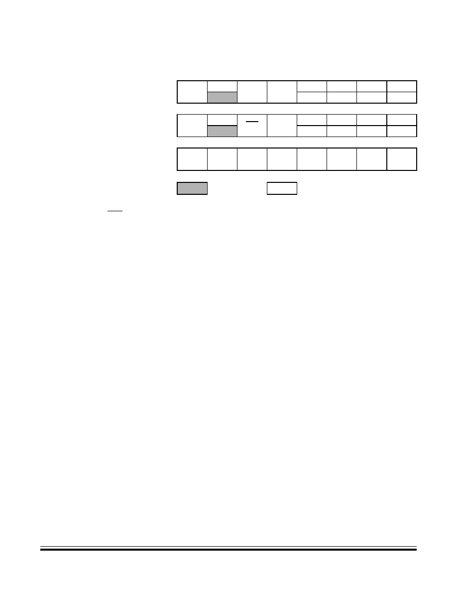
Addr.
Register Name
Bit 7
654321
Bit 0
$001C
PLL Control Register
(PCTL)
Read:
PLLIE
PLLF
PLLON
BCS
1111
Write:
RRRR
Reset:
00101111
$001D
PLL Bandwidth Control Register
(PBWC)
Read:
AUTO
LOCK
ACQ
XLD
0000
Write:
RRRR
Reset:
00000000
$001E
PLL Programming Register
(PPG)
Read:
MUL7
MUL6
MUL5
MUL4
VRS7
VRS6
VRS5
VRS4
Write:
Reset:
01100110
= Unimplemented
R
= Reserved
1. When AUTO = 0, PLLIE is forced to logic 0 and is read-only.
2. When AUTO = 0, PLLF and LOCK read as logic 0.
3. When AUTO = 1, ACQ is read-only.
4. When PLLON = 0 or VRS[7:4] = $0, BCS is forced to logic 0 and is read-only.
5. When PLLON = 1, the PLL programming register is read-only.
6. When BCS = 1, PLLON is forced set and is read-only.
Figure 5-2. CGM I/O Register Summary
相关PDF资料 |
PDF描述 |
|---|---|
| MC68HRC98JL3ECFA | 8-BIT, FLASH, 4 MHz, MICROCONTROLLER, PQFP48 |
| MC68HRC98JL3EMDW | 8-BIT, FLASH, 8 MHz, MICROCONTROLLER, PDSO28 |
| MC68HC05C9AFN | 8-BIT, MROM, 2.1 MHz, MICROCONTROLLER, PQCC44 |
| MC9S08GB32CFU | 8-BIT, FLASH, 20 MHz, MICROCONTROLLER, PQFP64 |
| MC9S12A128BCFU | 16-BIT, FLASH, 25 MHz, MICROCONTROLLER, PQFP80 |
相关代理商/技术参数 |
参数描述 |
|---|---|
| MC68HC08AZ0 | 制造商:MOTOROLA 制造商全称:Motorola, Inc 功能描述:Advance Information |
| MC68HC08AZ0CFU | 制造商:MOTOROLA 制造商全称:Motorola, Inc 功能描述:Advance Information |
| MC68HC08AZ16 | 制造商:MOTOROLA 制造商全称:Motorola, Inc 功能描述:HCMOS Microcontroller Unit |
| MC68HC08AZ24 | 制造商:MOTOROLA 制造商全称:Motorola, Inc 功能描述:HCMOS Microcontroller Unit |
| MC68HC08AZ32 | 制造商:FREESCALE 制造商全称:Freescale Semiconductor, Inc 功能描述:Advance Information |
发布紧急采购,3分钟左右您将得到回复。