- 您现在的位置:买卖IC网 > PDF目录80358 > MC68LC302PU16 (MOTOROLA INC) 32-BIT, 16.67 MHz, RISC MICROCONTROLLER, PQFP100 PDF资料下载
参数资料
| 型号: | MC68LC302PU16 |
| 厂商: | MOTOROLA INC |
| 元件分类: | 微控制器/微处理器 |
| 英文描述: | 32-BIT, 16.67 MHz, RISC MICROCONTROLLER, PQFP100 |
| 封装: | TQFP-100 |
| 文件页数: | 19/182页 |
| 文件大小: | 618K |
| 代理商: | MC68LC302PU16 |
第1页第2页第3页第4页第5页第6页第7页第8页第9页第10页第11页第12页第13页第14页第15页第16页第17页第18页当前第19页第20页第21页第22页第23页第24页第25页第26页第27页第28页第29页第30页第31页第32页第33页第34页第35页第36页第37页第38页第39页第40页第41页第42页第43页第44页第45页第46页第47页第48页第49页第50页第51页第52页第53页第54页第55页第56页第57页第58页第59页第60页第61页第62页第63页第64页第65页第66页第67页第68页第69页第70页第71页第72页第73页第74页第75页第76页第77页第78页第79页第80页第81页第82页第83页第84页第85页第86页第87页第88页第89页第90页第91页第92页第93页第94页第95页第96页第97页第98页第99页第100页第101页第102页第103页第104页第105页第106页第107页第108页第109页第110页第111页第112页第113页第114页第115页第116页第117页第118页第119页第120页第121页第122页第123页第124页第125页第126页第127页第128页第129页第130页第131页第132页第133页第134页第135页第136页第137页第138页第139页第140页第141页第142页第143页第144页第145页第146页第147页第148页第149页第150页第151页第152页第153页第154页第155页第156页第157页第158页第159页第160页第161页第162页第163页第164页第165页第166页第167页第168页第169页第170页第171页第172页第173页第174页第175页第176页第177页第178页第179页第180页第181页第182页
Signal Description
5-20
MC68LC302 REFERENCE MANUAL
MOTOROLA
Each of these four pins can be used either as a dedicated timer function or as a general-
purpose port B I/O port pin. Note that the timers do not require the use of external pins. The
input buffers have Schmitt triggers.
TIN1/PB3—Timer 1 Input
This input is used as a timer clock source for timer 1 or as a trigger for the timer 1 capture
register. TIN1 may also be used as the external clock source for any SCC baud rate gen-
erators.
TIN2/PB5—Timer 2 Input
This input can be used as a timer clock source for timer 2 or as a trigger for the timer 2
capture register.
TOUT2/PB6—Timer 2 Output
This output is used as an active-low pulse timeout or as an event overflow output (toggle)
from timer 2.
WDOG/PB7—Watchdog Output
This active-low, open-drain output indicates expiration of the watchdog timer. WDOG is
asserted for a period of 16 clock (CLKO) cycles and may be externally connected to the
RESET and HALT pins to reset the MC68LC302. The WDOG pin function is enabled after
a total system reset. It may be reassigned as the PB7 I/O pin in the PBCNT register.
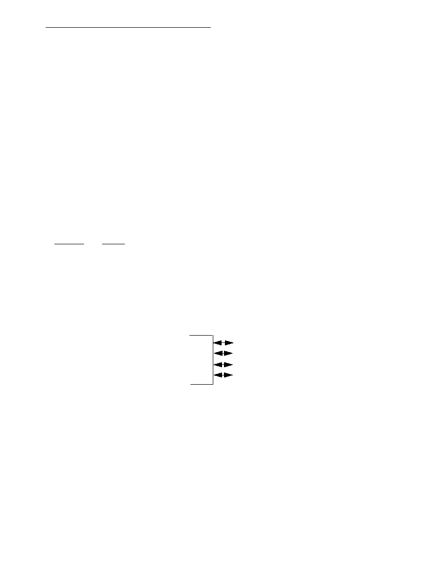
5.17 PARALLEL I/O PINS WITH INTERRUPT CAPABILITY
The four parallel I/O pins with interrupt are shown in Figure 5-13.
Figure 5-13. Port B Parallel I/O Pins with Interrupt
PB11–PB8—Port B Parallel I/O pins
These four pins may be configured as a general-purpose parallel I/O ports with interrupt ca-
pability. Each of the pins can be configured either as an input or an output. When configured
as an input, each pin can generate a separate, maskable interrupt on a high-to-low transi-
tion. PB8 may also be used to request a refresh cycle from the DRAM refresh controller rath-
er than as an I/O pin. The input buffers have Schmitt triggers.
PB8
PB9
PB10
PB11
相关PDF资料 |
PDF描述 |
|---|---|
| MC68HC11KA1VFN4 | 8-BIT, EEPROM, 4 MHz, MICROCONTROLLER, PQCC68 |
| MC68HC11KA3MFN4 | 8-BIT, MROM, 4 MHz, MICROCONTROLLER, PQCC68 |
| MC68B09ECP | 8-BIT, 2 MHz, MICROPROCESSOR, PDIP40 |
| M38B59EF-XXXFP | 8-BIT, OTPROM, 4.2 MHz, MICROCONTROLLER, PQFP80 |
| M37774M9XXXGP | 16-BIT, MROM, 16 MHz, MICROCONTROLLER, PQFP100 |
相关代理商/技术参数 |
参数描述 |
|---|---|
| MC68LC302PU16CT | 功能描述:IC MPU MULTI PROTOCOL 100-LQFP RoHS:否 类别:集成电路 (IC) >> 嵌入式 - 微处理器 系列:M683xx 标准包装:2 系列:MPC8xx 处理器类型:32-位 MPC8xx PowerQUICC 特点:- 速度:133MHz 电压:3.3V 安装类型:表面贴装 封装/外壳:357-BBGA 供应商设备封装:357-PBGA(25x25) 包装:托盘 |
| MC68LC302PU16VCT | 功能描述:IC MPU NETWORK 16MHZ 100-LQFP RoHS:否 类别:集成电路 (IC) >> 嵌入式 - 微处理器 系列:M683xx 标准包装:2 系列:MPC8xx 处理器类型:32-位 MPC8xx PowerQUICC 特点:- 速度:133MHz 电压:3.3V 安装类型:表面贴装 封装/外壳:357-BBGA 供应商设备封装:357-PBGA(25x25) 包装:托盘 |
| MC68LC302PU20CT | 功能描述:微处理器 - MPU 20MHz 2MIPS RoHS:否 制造商:Atmel 处理器系列:SAMA5D31 核心:ARM Cortex A5 数据总线宽度:32 bit 最大时钟频率:536 MHz 程序存储器大小:32 KB 数据 RAM 大小:128 KB 接口类型:CAN, Ethernet, LIN, SPI,TWI, UART, USB 工作电源电压:1.8 V to 3.3 V 最大工作温度:+ 85 C 安装风格:SMD/SMT 封装 / 箱体:FBGA-324 |
| MC68LC302PU20VCT | 功能描述:IC MPU NETWORK 20MHZ 100-LQFP RoHS:否 类别:集成电路 (IC) >> 嵌入式 - 微处理器 系列:M683xx 标准包装:2 系列:MPC8xx 处理器类型:32-位 MPC8xx PowerQUICC 特点:- 速度:133MHz 电压:3.3V 安装类型:表面贴装 封装/外壳:357-BBGA 供应商设备封装:357-PBGA(25x25) 包装:托盘 |
| MC68LC302PU25CT | 功能描述:微处理器 - MPU 25MHz 2.5MIPS RoHS:否 制造商:Atmel 处理器系列:SAMA5D31 核心:ARM Cortex A5 数据总线宽度:32 bit 最大时钟频率:536 MHz 程序存储器大小:32 KB 数据 RAM 大小:128 KB 接口类型:CAN, Ethernet, LIN, SPI,TWI, UART, USB 工作电源电压:1.8 V to 3.3 V 最大工作温度:+ 85 C 安装风格:SMD/SMT 封装 / 箱体:FBGA-324 |
发布紧急采购,3分钟左右您将得到回复。