参数资料
| 型号: | MC7410TVU400LE |
| 厂商: | Freescale Semiconductor |
| 文件页数: | 55/56页 |
| 文件大小: | 0K |
| 描述: | MPU RISC 32BIT 360-CBGA |
| 标准包装: | 44 |
| 系列: | MPC74xx |
| 处理器类型: | 32-位 MPC74xx PowerPC |
| 速度: | 400MHz |
| 电压: | 1.8V |
| 安装类型: | 表面贴装 |
| 封装/外壳: | 360-BCBGA,FCCBGA |
| 供应商设备封装: | 360-FCCBGA(25x25) |
| 包装: | 托盘 |
第1页第2页第3页第4页第5页第6页第7页第8页第9页第10页第11页第12页第13页第14页第15页第16页第17页第18页第19页第20页第21页第22页第23页第24页第25页第26页第27页第28页第29页第30页第31页第32页第33页第34页第35页第36页第37页第38页第39页第40页第41页第42页第43页第44页第45页第46页第47页第48页第49页第50页第51页第52页第53页第54页当前第55页第56页
MPC7410 RISC Microprocessor Hardware Specifications, Rev. 6.1
8
Freescale Semiconductor
Electrical and Thermal Characteristics
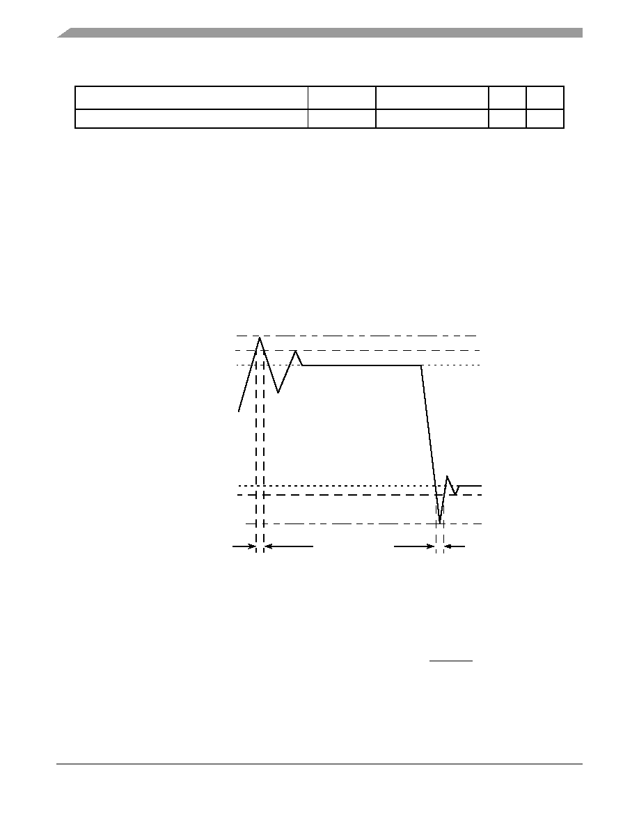
Figure 2 shows the allowable undershoot and overshoot voltage for the MPC7410.
Figure 2. Overshoot/Undershoot Voltage
The MPC7410 provides several I/O voltages to support both compatibility with existing systems and migration to
future systems. The MPC7410 core voltage must always be provided at nominal voltage (see Table 3 for actual
recommended core voltage). Voltage to the L2 I/Os and processor interface I/Os are provided through separate sets
of supply pins and may be provided at the voltages shown in Table 2. Voltage must be provided to the L2OVDD
power pins even if the interface is not used. The input voltage threshold for each bus is selected by sampling the
state of the voltage select pins BVSEL and L2VSEL at the negation of the signal HRESET. These signals must
remain stable during part operation and cannot change. The output voltage will swing from GND to the maximum
voltage applied to the OVDD or L2OVDD power pins.
Rework temperature
Trwk
260
°C
—
Notes:
1. Functional and tested operating conditions are given in Table 3. Absolute maximum ratings are stress ratings only,
and functional operation at the maximums is not guaranteed. Stresses beyond those listed may affect device
reliability or cause permanent damage to the device.
2. Caution: Vin must not exceed OVDD or L2OVDD by more than 0.2 V at any time including during power-on reset.
3. Caution: L2OVDD/OVDD must not exceed VDD/AVDD/L2AVDD by more than 2.0 V at any time including during
power-on reset; this limit may be exceeded for a maximum of 20 ms during power-on reset and power-down
sequences.
4. Caution: VDD/AVDD/L2AVDD must not exceed L2OVDD/OVDD by more than 0.4 V at any time including during
power-on reset; this limit may be exceeded for a maximum of 20 ms during power-on reset and power-down
sequences.
6. M
xx7410xxnnnLE (Rev. 1.4) and later only. Previous revisions do not support 3.3 V OVDD and have a maximum
value OVDD of –0.3 to 2.8 V.
Table 1. Absolute Maximum Ratings 1 (continued)
Characteristic
Symbol
Maximum Value
Unit
Notes
VIH
GND
GND – 0.3 V
GND – 0.7 V
Not to Exceed 10%
(L2)OVDD + 20%
VIL
(L2)OVDD
(L2)OVDD + 5%
of tSYSCLK (OVDD)
or tL2CLK (L2OVDD)
相关PDF资料 |
PDF描述 |
|---|---|
| IDT71T75802S166BGI8 | IC SRAM 18MBIT 166MHZ 119BGA |
| FMC35DRAI | CONN EDGECARD 70POS R/A .100 SLD |
| MPC8567EVTAQGG | MPU POWERQUICC III 1023-PBGA |
| IDT71T75802S166BGGI8 | IC SRAM 18MBIT 166MHZ 119BGA |
| FMM43DSEF-S13 | CONN EDGECARD 86POS .156 EXTEND |
相关代理商/技术参数 |
参数描述 |
|---|---|
| MC7410VU400LE | 功能描述:微处理器 - MPU REV 1.4 105C PB FREE RoHS:否 制造商:Atmel 处理器系列:SAMA5D31 核心:ARM Cortex A5 数据总线宽度:32 bit 最大时钟频率:536 MHz 程序存储器大小:32 KB 数据 RAM 大小:128 KB 接口类型:CAN, Ethernet, LIN, SPI,TWI, UART, USB 工作电源电压:1.8 V to 3.3 V 最大工作温度:+ 85 C 安装风格:SMD/SMT 封装 / 箱体:FBGA-324 |
| MC7410VU400NE | 功能描述:微处理器 - MPU NITRO RV 1.4 ROHS RoHS:否 制造商:Atmel 处理器系列:SAMA5D31 核心:ARM Cortex A5 数据总线宽度:32 bit 最大时钟频率:536 MHz 程序存储器大小:32 KB 数据 RAM 大小:128 KB 接口类型:CAN, Ethernet, LIN, SPI,TWI, UART, USB 工作电源电压:1.8 V to 3.3 V 最大工作温度:+ 85 C 安装风格:SMD/SMT 封装 / 箱体:FBGA-324 |
| MC7410VU450NE | 功能描述:微处理器 - MPU NITRO RV 1.4 ROHS RoHS:否 制造商:Atmel 处理器系列:SAMA5D31 核心:ARM Cortex A5 数据总线宽度:32 bit 最大时钟频率:536 MHz 程序存储器大小:32 KB 数据 RAM 大小:128 KB 接口类型:CAN, Ethernet, LIN, SPI,TWI, UART, USB 工作电源电压:1.8 V to 3.3 V 最大工作温度:+ 85 C 安装风格:SMD/SMT 封装 / 箱体:FBGA-324 |
| MC7410VU500LE | 功能描述:微处理器 - MPU REV 1.4 105C PB FREE RoHS:否 制造商:Atmel 处理器系列:SAMA5D31 核心:ARM Cortex A5 数据总线宽度:32 bit 最大时钟频率:536 MHz 程序存储器大小:32 KB 数据 RAM 大小:128 KB 接口类型:CAN, Ethernet, LIN, SPI,TWI, UART, USB 工作电源电压:1.8 V to 3.3 V 最大工作温度:+ 85 C 安装风格:SMD/SMT 封装 / 箱体:FBGA-324 |
| MC7411MEL | 制造商:Rochester Electronics LLC 功能描述:- Bulk |
发布紧急采购,3分钟左右您将得到回复。