- 您现在的位置:买卖IC网 > PDF目录4059 > MC7447AVU600NB (Freescale Semiconductor)IC MPU RISC 32BIT 360-BGA PDF资料下载
参数资料
| 型号: | MC7447AVU600NB |
| 厂商: | Freescale Semiconductor |
| 文件页数: | 9/56页 |
| 文件大小: | 0K |
| 描述: | IC MPU RISC 32BIT 360-BGA |
| 标准包装: | 44 |
| 系列: | MPC74xx |
| 处理器类型: | 32-位 MPC74xx PowerPC |
| 速度: | 600MHz |
| 电压: | 1.1V |
| 安装类型: | 表面贴装 |
| 封装/外壳: | 360-BCBGA,FCCBGA |
| 供应商设备封装: | 360-FCCBGA(25x25) |
| 包装: | 托盘 |
第1页第2页第3页第4页第5页第6页第7页第8页当前第9页第10页第11页第12页第13页第14页第15页第16页第17页第18页第19页第20页第21页第22页第23页第24页第25页第26页第27页第28页第29页第30页第31页第32页第33页第34页第35页第36页第37页第38页第39页第40页第41页第42页第43页第44页第45页第46页第47页第48页第49页第50页第51页第52页第53页第54页第55页第56页
MPC7447A RISC Microprocessor Hardware Specifications, Rev. 5
Freescale Semiconductor
17
Electrical and Thermal Characteristics
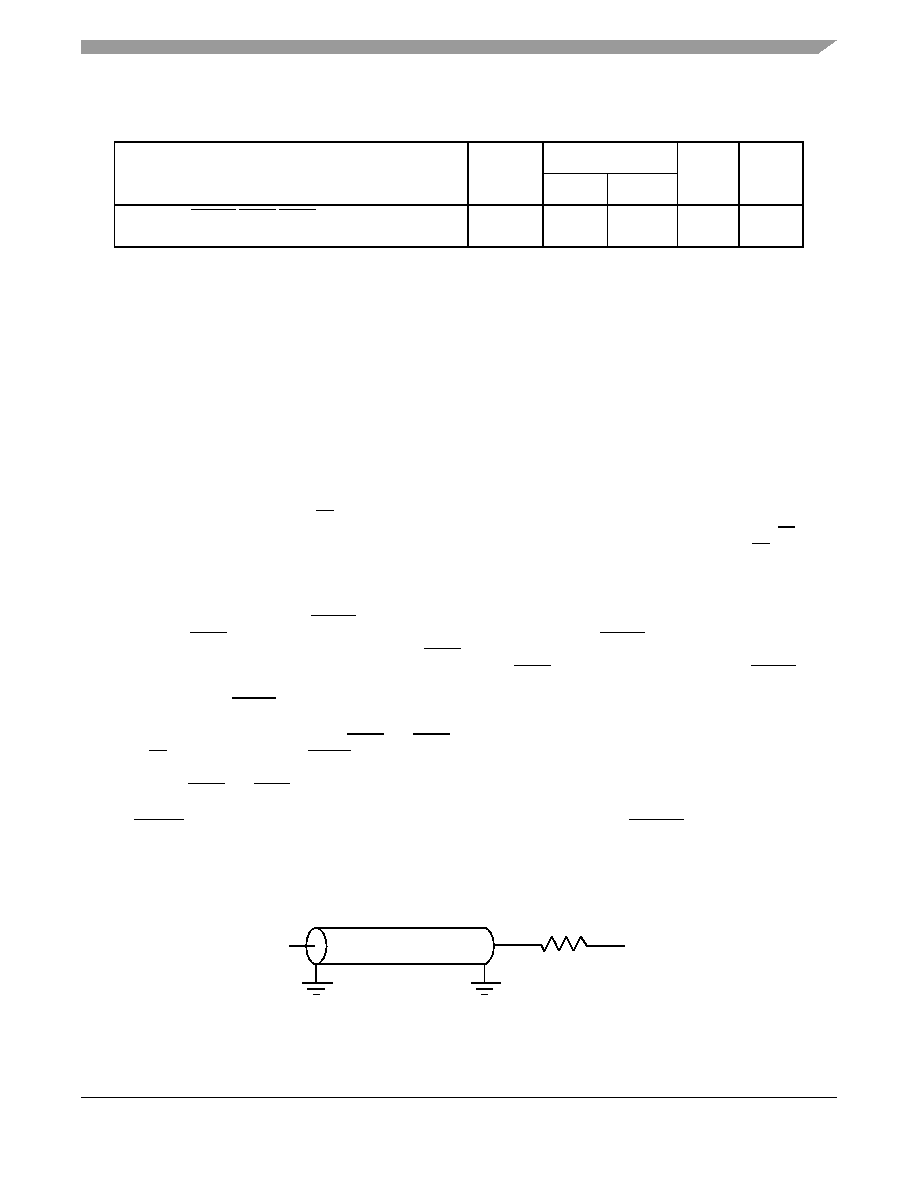
Figure 4 provides the AC test load for the MPC7447A.
Figure 4. AC Test Load
SYSCLK to ARTRY/SHD0/SHD1 high impedance after
precharge
tKHARPZ
—2
tSYSCLK 3, 5, 6, 7
Notes:
1. All input specifications are measured from the midpoint of the signal in question to the midpoint of the rising edge
of the input SYSCLK. All output specifications are measured from the midpoint of the rising edge of SYSCLK to
the midpoint of the signal in question. All output timings assume a purely resistive 50-
Ω load (see Figure 4). Input
and output timings are measured at the pin; time-of-flight delays must be added for trace lengths, vias, and
connectors in the system.
2. The symbology used for timing specifications herein follows the pattern of t(signal)(state)(reference)(state) for inputs
and t(reference)(state)(signal)(state) for outputs. For example, tIVKH symbolizes the time input signals (I) reach the valid
state (V) relative to the SYSCLK reference (K) going to the high (H) state or input setup time. And tKHOV
symbolizes the time from SYSCLK(K) going high (H) until outputs (O) are valid (V) or output valid time. Input hold
time can be read as the time that the input signal (I) went invalid (X) with respect to the rising clock edge (KH)
(note the position of the reference and its state for inputs) and output hold time can be read as the time from the
rising edge (KH) until the output went invalid (OX).
3. tsysclk is the period of the external clock (SYSCLK) in ns. The numbers given in the table must be multiplied by
the period of SYSCLK to compute the actual time duration (in ns) of the parameter in question.
4. According to the bus protocol, TS is driven only by the currently active bus master. It is asserted low and
precharged high before returning to high impedance, as shown in Figure 6. The nominal precharge width for TS
is 0.5
× tSYSCLK, that is, less than the minimum tSYSCLK period, to ensure that another master asserting TS on
the following clock will not contend with the precharge. Output valid and output hold timing is tested for the signal
asserted. Output valid time is tested for precharge.The high-impedance behavior is guaranteed by design.
5. Guaranteed by design and not tested.
6. According to the bus protocol, ARTRY can be driven by multiple bus masters through the clock period immediately
following AACK. Bus contention is not an issue because any master asserting ARTRY will be driving it low. Any
master asserting it low in the first clock following AACK will then go to high impedance for 1 clock before
precharging it high during the second cycle after the assertion of AACK. The nominal precharge width for ARTRY
is 1.0 tSYSCLK; that is, it should be high impedance as shown in Figure 6 before the first opportunity for another
master to assert ARTRY. Output valid and output hold timing is tested for the signal asserted.The high-impedance
behavior is guaranteed by design.
7. According to the MPX bus protocol, SHD0 and SHD1 can be driven by multiple bus masters beginning the cycle
of TS. Timing is the same as ARTRY, that is, the signal is high impedance for a fraction of a cycle, then negated
for up to an entire cycle (crossing a bus cycle boundary) before being three-stated again. The nominal precharge
width for SHD0 and SHD1 is 1.0 tSYSCLK. The edges of the precharge vary depending on the programmed ratio
of core to bus (PLL configurations).
8. BMODE[0:1] and BVSEL are mode select inputs and are sampled before and after HRESET negation. These
parameters represent the input setup and hold times for each sample. These values are guaranteed by design
and not tested. These inputs must remain stable after the second sample. See Figure 5 for sample timing.
Table 9. Processor Bus AC Timing Specifications1 (continued)
At recommended operating conditions. See Table 4.
Parameter
Symbol 2
All Speed Grades
Unit
Notes
Min
Max
Output
Z0 = 50 Ω
OVDD/2
RL = 50 Ω
相关PDF资料 |
PDF描述 |
|---|---|
| AMC65DRTS-S13 | CONN EDGECARD 130POS .100 EXTEND |
| MPC8275CZQMIBA | IC MPU POWERQUICC II 516-PBGA |
| AMC65DRES-S13 | CONN EDGECARD 130POS .100 EXTEND |
| XF2M-3315-1A | CONN FPC 33POS 0.5MM PITCH SMD |
| AMC50DRYN-S93 | CONN EDGECARD 100PS DIP .100 SLD |
相关代理商/技术参数 |
参数描述 |
|---|---|
| MC7447AVU733NB | 功能描述:微处理器 - MPU A7PM PB FREE RoHS:否 制造商:Atmel 处理器系列:SAMA5D31 核心:ARM Cortex A5 数据总线宽度:32 bit 最大时钟频率:536 MHz 程序存储器大小:32 KB 数据 RAM 大小:128 KB 接口类型:CAN, Ethernet, LIN, SPI,TWI, UART, USB 工作电源电压:1.8 V to 3.3 V 最大工作温度:+ 85 C 安装风格:SMD/SMT 封装 / 箱体:FBGA-324 |
| MC7447AVU867NB | 功能描述:微处理器 - MPU A7PM PB FREE SPHERES RoHS:否 制造商:Atmel 处理器系列:SAMA5D31 核心:ARM Cortex A5 数据总线宽度:32 bit 最大时钟频率:536 MHz 程序存储器大小:32 KB 数据 RAM 大小:128 KB 接口类型:CAN, Ethernet, LIN, SPI,TWI, UART, USB 工作电源电压:1.8 V to 3.3 V 最大工作温度:+ 85 C 安装风格:SMD/SMT 封装 / 箱体:FBGA-324 |
| MC7447RX1000LB | 制造商:Motorola Inc 功能描述: |
| MC7447RX1000NB | 制造商:Freescale Semiconductor 功能描述:IC, 32BIT MPU, 1000MHZ, BGA-360, Series:(Power) HOST MPU, Core Size:32bit, Progr |
| MC7447RX600NB | 制造商:MOTOROLA 制造商全称:Motorola, Inc 功能描述:PPC7457RX1000NB |
发布紧急采购,3分钟左右您将得到回复。