参数资料
| 型号: | MC74AC273NG |
| 厂商: | ON Semiconductor |
| 文件页数: | 1/8页 |
| 文件大小: | 0K |
| 描述: | IC FLIP FLOP D OCTAL CMOS 20DIP |
| 标准包装: | 18 |
| 系列: | 74AC |
| 功能: | 主复位 |
| 类型: | D 型总线 |
| 输出类型: | 非反相 |
| 元件数: | 1 |
| 每个元件的位元数: | 8 |
| 频率 - 时钟: | 175MHz |
| 延迟时间 - 传输: | 5.5ns |
| 触发器类型: | 正边沿 |
| 输出电流高,低: | 24mA,24mA |
| 电源电压: | 2 V ~ 6 V |
| 工作温度: | -40°C ~ 85°C |
| 安装类型: | 通孔 |
| 封装/外壳: | 20-DIP(0.300",7.62mm) |
| 包装: | 管件 |
| 其它名称: | MC74AC273NGOS |
Semiconductor Components Industries, LLC, 2005
December, 2005 Rev. 6
1
Publication Order Number:
MC74AC273/D
MC74AC273, MC74ACT273
Octal D FlipFlop
The MC74AC273/74ACT273 has eight edge-triggered Dtype
flipflops with individual D inputs and Q outputs. The common
buffered Clock (CP) and Master Reset (MR) inputs load and reset
(clear) all flipflops simultaneously.
The register is fully edge-triggered. The state of each D input, one
setup time before the LOWtoHIGH clock transition, is transferred
to the corresponding flipflop’s Q output.
All outputs will be forced LOW independently of Clock or Data
inputs by a LOW voltage level on the MR input. The device is useful
for applications where the true output only is required and the Clock
and Master Reset are common to all storage elements.
Features
Ideal Buffer for MOS Microprocessor or Memory
Eight Edge-Triggered D FlipFlops
Buffered Common Clock
Buffered, Asynchronous Master Reset
See MC74AC377 for Clock Enable Version
See MC74AC373 for Transparent Latch Version
See MC74AC374 for 3-State Version
Outputs Source/Sink 24 mA
′ACT273 Has TTL Compatible Inputs
PbFree Packages are Available*
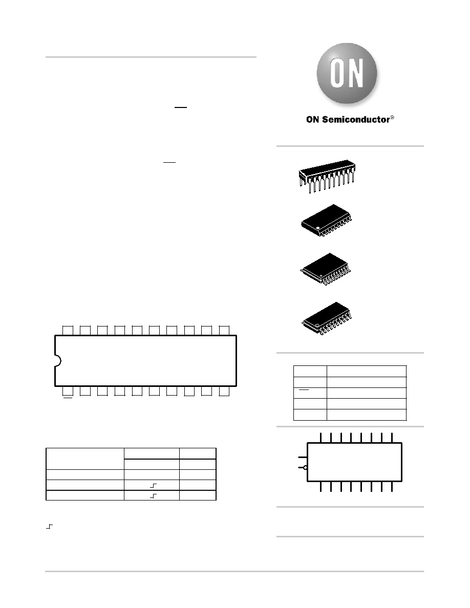
Pinout: 20Lead Packages Conductors
19
20
18
17
16
15
14
2
1
34567
VCC
13
8
12
9
11
10
Q7
D7
D6
Q6
Q5
D5
D4
Q4
CP
MR
Q0
D0
D1
Q1
Q2
D2
D3
Q3 GND
(Top View)
MODE SELECT-FUNCTION TABLE
Operating Mode
Inputs
Outputs
MR
CP
Dn
Qn
Reset (Clear)
L
X
L
Load
′1′
H
Load
′0′
H
L
H = HIGH Voltage Level
L = LOW Voltage Level
X = Immaterial
= LOW-to-HIGH Clock Transition
*For additional information on our PbFree strategy and soldering details, please
download the ON Semiconductor Soldering and Mounting Techniques
Reference Manual, SOLDERRM/D.
SOEIAJ20
SUFFIX M
CASE 967
http://onsemi.com
See detailed ordering and shipping information in the package
dimensions section on page 5 of this data sheet.
ORDERING INFORMATION
1
TSSOP20
SUFFIX DT
CASE 948E
SOIC20WB
SUFFIX DW
CASE 751D
1
See general marking information in the device marking
section on page 6 of this data sheet.
DEVICE MARKING INFORMATION
20
PDIP20
SUFFIX N
CASE 738
1
20
PIN ASSIGNMENT
PIN
D0D7
FUNCTION
Data Inputs
MR
Master Reset
CP
Clock Pulse Input
Q0Q7
Data Outputs
Q0 Q1 Q2 Q3 Q4 Q5 Q6 Q7
D0 D1 D2 D3 D4 D5 D6 D7
CP
MR
Logic Symbol
相关PDF资料 |
PDF描述 |
|---|---|
| VE-210-MV-F1 | CONVERTER MOD DC/DC 5V 150W |
| MS27467T21B35PALC | CONN HSG PLUG 79POS STRGHT PIN |
| VI-26X-MV-F4 | CONVERTER MOD DC/DC 5.2V 150W |
| 74LVT16374MTD | IC FLIP FLOP 16BIT D 3ST 48TSSOP |
| VI-26X-MV-F2 | CONVERTER MOD DC/DC 5.2V 150W |
相关代理商/技术参数 |
参数描述 |
|---|---|
| MC74AC299 | 制造商:ONSEMI 制造商全称:ON Semiconductor 功能描述:8-Input Universal Shift/ Storage Register with Common Parallel I/O Pins |
| MC74AC299DW | 制造商:ONSEMI 制造商全称:ON Semiconductor 功能描述:8-Input Universal Shift/ Storage Register with Common Parallel I/O Pins |
| MC74AC299DWR2 | 制造商:ONSEMI 制造商全称:ON Semiconductor 功能描述:8-Input Universal Shift/ Storage Register with Common Parallel I/O Pins |
| MC74AC299N | 制造商:ONSEMI 制造商全称:ON Semiconductor 功能描述:8-Input Universal Shift/ Storage Register with Common Parallel I/O Pins |
| MC74AC32 | 制造商:ONSEMI 制造商全称:ON Semiconductor 功能描述:QUAD 2-INPUT OR GATE |
发布紧急采购,3分钟左右您将得到回复。