参数资料
| 型号: | MC74AC273NG |
| 厂商: | ON Semiconductor |
| 文件页数: | 3/8页 |
| 文件大小: | 0K |
| 描述: | IC FLIP FLOP D OCTAL CMOS 20DIP |
| 标准包装: | 18 |
| 系列: | 74AC |
| 功能: | 主复位 |
| 类型: | D 型总线 |
| 输出类型: | 非反相 |
| 元件数: | 1 |
| 每个元件的位元数: | 8 |
| 频率 - 时钟: | 175MHz |
| 延迟时间 - 传输: | 5.5ns |
| 触发器类型: | 正边沿 |
| 输出电流高,低: | 24mA,24mA |
| 电源电压: | 2 V ~ 6 V |
| 工作温度: | -40°C ~ 85°C |
| 安装类型: | 通孔 |
| 封装/外壳: | 20-DIP(0.300",7.62mm) |
| 包装: | 管件 |
| 其它名称: | MC74AC273NGOS |
MC74AC273, MC74ACT273
http://onsemi.com
3
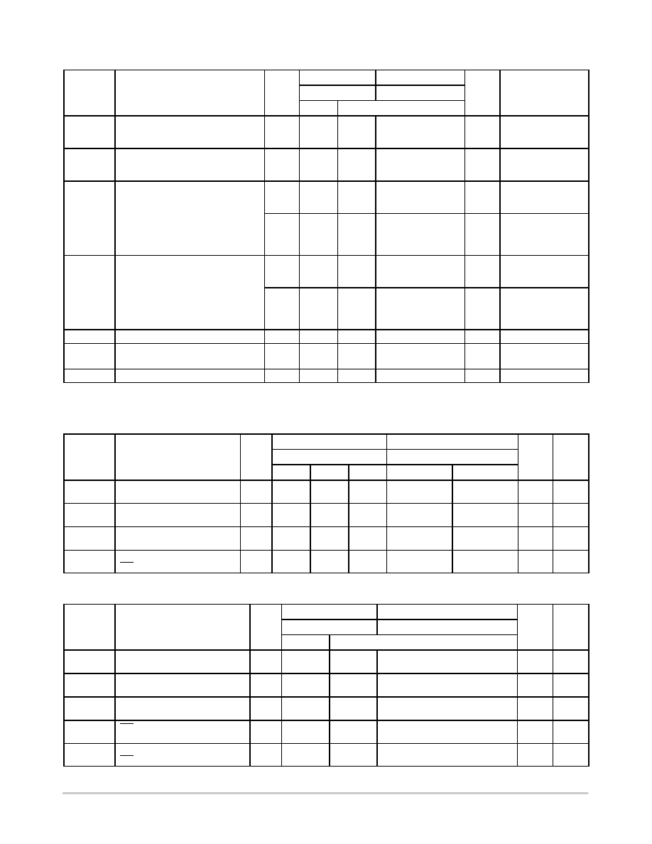
DC CHARACTERISTICS
Symbol
Parameter
VCC
(V)
74AC
Unit
Conditions
TA = +25°C
TA = 40°C to +85°C
Typ
Guaranteed Limits
VIH
Minimum High Level Input Voltage
3.0
4.5
5.5
1.5
2.25
2.75
2.1
3.15
3.85
2.1
3.15
3.85
V
VOUT = 0.1 V
or VCC 0.1 V
VIL
Maximum Low Level Input Voltage
3.0
4.5
5.5
1.5
2.25
2.75
0.9
1.35
1.65
0.9
1.35
1.65
V
VOUT = 0.1 V
or VCC 0.1 V
VOH
Minimum High Level Output Voltage
3.0
4.5
5.5
2.99
4.49
5.49
2.9
4.4
5.4
2.9
4.4
5.4
V
IOUT = 50 mA
3.0
4.5
5.5
2.56
3.86
4.86
2.46
3.76
4.76
V
*VIN = VIL or VIH
12 mA
IOH
24 mA
VOL
Maximum Low Level Output Voltage
3.0
4.5
5.5
0.002
0.001
0.1
V
IOUT = 50 mA
3.0
4.5
5.5
0.36
0.44
V
*VIN = VIL or VIH
12 mA
IOL
24 mA
IIN
Maximum Input Leakage Current
5.5
±0.1
±1.0
mA
VI = VCC, GND
IOLD
IOHD
Minimum Dynamic Output Current
5.5
75
mA
VOLD = 1.65 V Max
VOHD = 3.85 V Min
ICC
Maximum Quiescent Supply Current
5.5
8.0
80
mA
VIN = VCC or GND
*All outputs loaded; thresholds on input associated with output under test.
Maximum test duration 2.0 ms, one output loaded at a time.
NOTE:
Note: IIN and ICC @ 3.0 V are guaranteed to be less than or equal to the respective limit @ 5.5 V VCC.
AC CHARACTERISTICS (For Figures and Waveforms See Section 3 of the ON Semiconductor FACT Data Book, DL138/D)
Symbol
Parameter
VCC*
(V)
74AC
Unit
Figure
No.
TA = +25°C CL = 50 pF
TA = 40°C to +85°C CL = 50 pF
Min
Typ
Max
Min
Max
fmax
Maximum Clock
Frequency
3.3
5.0
90
140
125
175
75
125
Mhz
33
tPLH
Propagation Delay
Clock to Output
3.3
5.0
4.0
3.0
7.0
5.5
12.5
9.0
3.0
2.5
14.0
10.0
ns
36
tPHL
Propagation Delay
Clock to Output
3.3
5.0
4.0
3.0
7.0
5.0
13.0
10.0
3.5
2.5
14.5
11.0
ns
36
tPHL
Propagation Delay
MR to Output
3.3
5.0
4.0
3.0
7.0
5.0
13.0
10.0
3.5
2.5
14.0
10.5
ns
36
*Voltage Range 3.3 V is 3.3 V
±0.3 V. Voltage Range 5.0 V is 5.0 V ±0.5 V.
AC OPERATING REQUIREMENTS
Symbol
Parameter
VCC*
(V)
74AC
Unit
Figure
No.
TA = +25°C CL = 50 pF
TA = 40°C to +85°C CL = 50 pF
Typ
Guaranteed Minimum
ts
Setup Time, HIGH or LOW
Data to CP
3.3
5.0
3.5
2.5
5.5
4.0
6.0
4.5
ns
39
th
Hold Time, HIGH or LOW
Data to CP
3.3
5.0
2.0
1.0
0
1.0
0
1.0
ns
39
tw
Clock Pulse Width
HIGH or LOW
3.3
5.0
3.5
2.5
5.5
4.0
6.0
4.5
ns
36
tw
MR Pulse Width
HIGH or LOW
3.3
5.0
2.0
1.5
5.5
4.0
6.0
4.5
ns
36
trec
Recovery Time
MR to CP
3.3
5.0
1.5
1.0
3.5
2.0
4.5
3.0
ns
39
*Voltage Range 3.3 V is 3.3 V
±0.3 V. Voltage Range 5.0 V is 5.0 V ±0.5 V.
相关PDF资料 |
PDF描述 |
|---|---|
| VE-210-MV-F1 | CONVERTER MOD DC/DC 5V 150W |
| MS27467T21B35PALC | CONN HSG PLUG 79POS STRGHT PIN |
| VI-26X-MV-F4 | CONVERTER MOD DC/DC 5.2V 150W |
| 74LVT16374MTD | IC FLIP FLOP 16BIT D 3ST 48TSSOP |
| VI-26X-MV-F2 | CONVERTER MOD DC/DC 5.2V 150W |
相关代理商/技术参数 |
参数描述 |
|---|---|
| MC74AC299 | 制造商:ONSEMI 制造商全称:ON Semiconductor 功能描述:8-Input Universal Shift/ Storage Register with Common Parallel I/O Pins |
| MC74AC299DW | 制造商:ONSEMI 制造商全称:ON Semiconductor 功能描述:8-Input Universal Shift/ Storage Register with Common Parallel I/O Pins |
| MC74AC299DWR2 | 制造商:ONSEMI 制造商全称:ON Semiconductor 功能描述:8-Input Universal Shift/ Storage Register with Common Parallel I/O Pins |
| MC74AC299N | 制造商:ONSEMI 制造商全称:ON Semiconductor 功能描述:8-Input Universal Shift/ Storage Register with Common Parallel I/O Pins |
| MC74AC32 | 制造商:ONSEMI 制造商全称:ON Semiconductor 功能描述:QUAD 2-INPUT OR GATE |
发布紧急采购,3分钟左右您将得到回复。