- 您现在的位置:买卖IC网 > PDF目录80429 > MC9S08RD16CDWE (FREESCALE SEMICONDUCTOR INC) 8-BIT, FLASH, 8 MHz, MICROCONTROLLER, PDSO28 PDF资料下载
参数资料
| 型号: | MC9S08RD16CDWE |
| 厂商: | FREESCALE SEMICONDUCTOR INC |
| 元件分类: | 微控制器/微处理器 |
| 英文描述: | 8-BIT, FLASH, 8 MHz, MICROCONTROLLER, PDSO28 |
| 封装: | ROHS COMPLIANT, MS-013AE, SOIC-28 |
| 文件页数: | 60/234页 |
| 文件大小: | 1758K |
| 代理商: | MC9S08RD16CDWE |
第1页第2页第3页第4页第5页第6页第7页第8页第9页第10页第11页第12页第13页第14页第15页第16页第17页第18页第19页第20页第21页第22页第23页第24页第25页第26页第27页第28页第29页第30页第31页第32页第33页第34页第35页第36页第37页第38页第39页第40页第41页第42页第43页第44页第45页第46页第47页第48页第49页第50页第51页第52页第53页第54页第55页第56页第57页第58页第59页当前第60页第61页第62页第63页第64页第65页第66页第67页第68页第69页第70页第71页第72页第73页第74页第75页第76页第77页第78页第79页第80页第81页第82页第83页第84页第85页第86页第87页第88页第89页第90页第91页第92页第93页第94页第95页第96页第97页第98页第99页第100页第101页第102页第103页第104页第105页第106页第107页第108页第109页第110页第111页第112页第113页第114页第115页第116页第117页第118页第119页第120页第121页第122页第123页第124页第125页第126页第127页第128页第129页第130页第131页第132页第133页第134页第135页第136页第137页第138页第139页第140页第141页第142页第143页第144页第145页第146页第147页第148页第149页第150页第151页第152页第153页第154页第155页第156页第157页第158页第159页第160页第161页第162页第163页第164页第165页第166页第167页第168页第169页第170页第171页第172页第173页第174页第175页第176页第177页第178页第179页第180页第181页第182页第183页第184页第185页第186页第187页第188页第189页第190页第191页第192页第193页第194页第195页第196页第197页第198页第199页第200页第201页第202页第203页第204页第205页第206页第207页第208页第209页第210页第211页第212页第213页第214页第215页第216页第217页第218页第219页第220页第221页第222页第223页第224页第225页第226页第227页第228页第229页第230页第231页第232页第233页第234页
Serial Communications Interface (S08SCIV1)
MC9S08RC/RD/RE/RG Data Sheet, Rev. 1.11
152
Freescale Semiconductor
12.2.3
SCI Control Register 2 (SCI1C2)
This register can be read or written at any time.
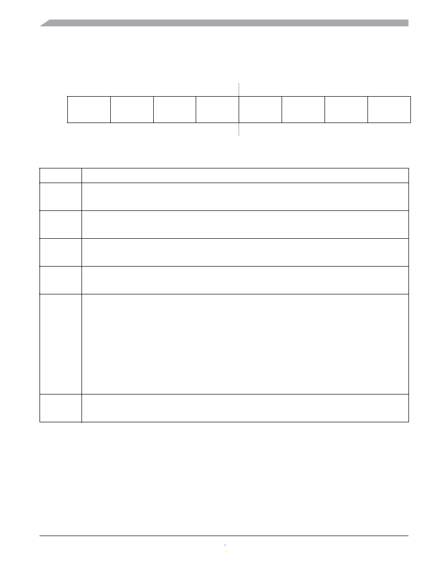
76543210
R
W
Reset
00000000
Figure 12-6. SCI Control Register 2 (SCI1C2)
Table 12-4. SCI1C2 Register Field Descriptions
Field
Description
7
TIE
Transmit Interrupt Enable (for TDRE)
0 Hardware interrupts from TDRE disabled (use polling).
1 Hardware interrupt requested when TDRE ag is 1.
6
TCIE
Transmission Complete Interrupt Enable (for TC)
0 Hardware interrupt requested when TC ag is 1.
1 Hardware interrupts from TC disabled (use polling).
5
RIE
Receiver Interrupt Enable (for RDRF)
0 Hardware interrupts from RDRF disabled (use polling).
1 Hardware interrupt requested when RDRF ag is 1.
4
ILIE
Idle Line Interrupt Enable (for IDLE)
0 Hardware interrupts from IDLE disabled (use polling).
1 Hardware interrupt requested when IDLE ag is 1.
3
TE
Transmitter Enable
0 Transmitter off.
1 Transmitter on.
TE must be 1 in order to use the SCI transmitter. Normally, when TE = 1, the SCI forces the TxD pin to act as an
output for the SCI system. If LOOPS = 1 and RSRC = 0, the TxD pin reverts to being a port B general-purpose
I/O pin even if TE = 1.
When the SCI is congured for single-wire operation (LOOPS = RSRC = 1), TXDIR controls the direction of
trafc on the single SCI communication line (TxD pin).
TE also can be used to queue an idle character by writing TE = 0 then TE = 1 while a transmission is in progress.
Refer to Section 12.3.2.1, “Send Break and Queued Idle,” for more details.
When TE is written to 0, the transmitter keeps control of the port TxD pin until any data, queued idle, or queued
break character nishes transmitting before allowing the pin to revert to a general-purpose I/O pin.
2
RE
Receiver Enable — When the SCI receiver is off, the RxD pin reverts to being a general-purpose port I/O pin.
0 Receiver off.
1 Receiver on.
相关PDF资料 |
PDF描述 |
|---|---|
| MC9S08RD32FJ | 8-BIT, FLASH, 8 MHz, MICROCONTROLLER, PQFP32 |
| MC68HC11E20CFU3 | 8-BIT, MROM, 3 MHz, MICROCONTROLLER, PQFP64 |
| MC68HC908QT4VFQ | 8-BIT, FLASH, 8 MHz, MICROCONTROLLER, DSO8 |
| MC68L11E1B2 | 8-BIT, 2 MHz, MICROCONTROLLER, PDIP56 |
| MC68020RC16E | 32-BIT, 16.67 MHz, MICROPROCESSOR, CPGA114 |
相关代理商/技术参数 |
参数描述 |
|---|---|
| MC9S08RD16CFDE | 制造商:FREESCALE 制造商全称:Freescale Semiconductor, Inc 功能描述:Microcontrollers |
| MC9S08RD16CFG | 制造商:Rochester Electronics LLC 功能描述:- Bulk |
| MC9S08RD16CFGE | 制造商:FREESCALE 制造商全称:Freescale Semiconductor, Inc 功能描述:Microcontrollers |
| MC9S08RD16CFJ | 制造商:Rochester Electronics LLC 功能描述:- Bulk |
| MC9S08RD16CFJE | 制造商:FREESCALE 制造商全称:Freescale Semiconductor, Inc 功能描述:Microcontrollers |
发布紧急采购,3分钟左右您将得到回复。