- 您现在的位置:买卖IC网 > PDF目录10958 > MCF5212LCVM66J (Freescale Semiconductor)IC MCU 256K FLASH 66MHZ 81MAPBGA PDF资料下载
参数资料
| 型号: | MCF5212LCVM66J |
| 厂商: | Freescale Semiconductor |
| 文件页数: | 27/56页 |
| 文件大小: | 0K |
| 描述: | IC MCU 256K FLASH 66MHZ 81MAPBGA |
| 标准包装: | 240 |
| 系列: | MCF521x |
| 核心处理器: | Coldfire V2 |
| 芯体尺寸: | 32-位 |
| 速度: | 66MHz |
| 连通性: | I²C,SPI,UART/USART |
| 外围设备: | DMA,LVD,POR,PWM,WDT |
| 输入/输出数: | 56 |
| 程序存储器容量: | 256KB(256K x 8) |
| 程序存储器类型: | 闪存 |
| RAM 容量: | 32K x 8 |
| 电压 - 电源 (Vcc/Vdd): | 3 V ~ 3.6 V |
| 数据转换器: | A/D 8x12b |
| 振荡器型: | 内部 |
| 工作温度: | -40°C ~ 85°C |
| 封装/外壳: | 81-LBGA |
| 包装: | 托盘 |
第1页第2页第3页第4页第5页第6页第7页第8页第9页第10页第11页第12页第13页第14页第15页第16页第17页第18页第19页第20页第21页第22页第23页第24页第25页第26页当前第27页第28页第29页第30页第31页第32页第33页第34页第35页第36页第37页第38页第39页第40页第41页第42页第43页第44页第45页第46页第47页第48页第49页第50页第51页第52页第53页第54页第55页第56页
Electrical Characteristics
MCF5213 ColdFire Microcontroller, Rev. 3
Freescale Semiconductor
33
2.8
General Purpose I/O Timing
GPIO can be configured for certain pins of the QSPI, DDR Control, timer, UART, and Interrupt interfaces. When in GPIO mode,
The GPIO timing is met under the following load test conditions:
50 pF / 50
Ω for high drive
25 pF / 25
Ω for low drive
Frequency un-LOCK range
fUL
–1.5
1.5
% fref
Frequency LOCK range
fLCK
–0.75
0.75
% fref
CLKOUT period jitter 4, 5, 8 ,9, measured at fSYS Max
Peak-to-peak (clock edge to clock edge)
Long term (averaged over 2 ms interval)
Cjitter
—
10
.01
% fsys
On-chip oscillator frequency
foco
7.84
8.16
MHz
1 All internal registers retain data at 0 Hz.
2 Depending on packaging; see Table 2.
3 Loss of Reference Frequency is the reference frequency detected internally, which transitions the PLL into self clocked mode.
4 Self clocked mode frequency is the frequency at which the PLL operates when the reference frequency falls below f
LOR with
default MFD/RFD settings.
5 This parameter is characterized before qualification rather than 100% tested.
6 Proper PC board layout procedures must be followed to achieve specifications.
7 This specification applies to the period required for the PLL to relock after changing the MFD frequency control bits in the
synthesizer control register (SYNCR).
8 Jitter is the average deviation from the programmed frequency measured over the specified interval at maximum f
sys.
Measurements are made with the device powered by filtered supplies and clocked by a stable external clock signal. Noise
injected into the PLL circuitry via VDDPLL and VSSPLL and variation in crystal oscillator frequency increase the Cjitter percentage
for a given interval.
9 Based on slow system clock of 40 MHz measured at f
sys max.
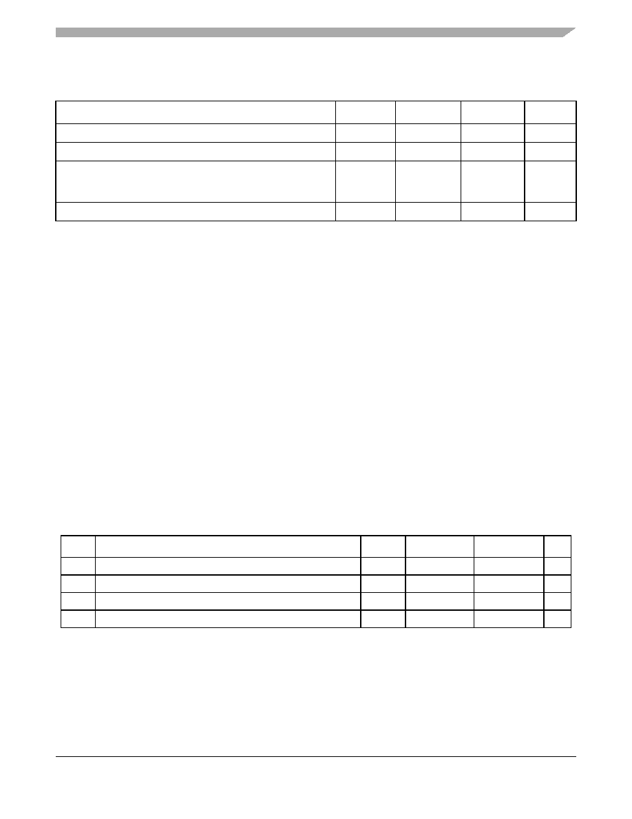
Table 28. GPIO Timing
NUM
Characteristic
Symbol
Min
Max
Unit
G1
CLKOUT High to GPIO Output Valid
tCHPOV
—10
ns
G2
CLKOUT High to GPIO Output Invalid
tCHPOI
1.5
—
ns
G3
GPIO Input Valid to CLKOUT High
tPVCH
9—
ns
G4
CLKOUT High to GPIO Input Invalid
tCHPI
1.5
—
ns
Table 27. PLL Electrical Specifications (continued)
(VDD and VDDPLL = 2.7 to 3.6 V, VSS = VSSPLL = 0 V)
Characteristic
Symbol
Min
Max
Unit
相关PDF资料 |
PDF描述 |
|---|---|
| VI-BTV-IW-B1 | CONVERTER MOD DC/DC 5.8V 100W |
| PKG.M1.0SL.LG | CONN RCPT 10POS PNL MNT SKT SLDR |
| MCF5212LCVM66 | IC MCU 256K FLASH 66MHZ 81MAPBGA |
| VI-BTT-IX-B1 | CONVERTER MOD DC/DC 6.5V 75W |
| UTS612E4S | CONN PLUG 4POS W/O BKSHLL W/SKT |
相关代理商/技术参数 |
参数描述 |
|---|---|
| MCF5212LCVM80 | 功能描述:32位微控制器 - MCU MCF5212 KIRIN RoHS:否 制造商:Texas Instruments 核心:C28x 处理器系列:TMS320F28x 数据总线宽度:32 bit 最大时钟频率:90 MHz 程序存储器大小:64 KB 数据 RAM 大小:26 KB 片上 ADC:Yes 工作电源电压:2.97 V to 3.63 V 工作温度范围:- 40 C to + 105 C 封装 / 箱体:LQFP-80 安装风格:SMD/SMT |
| MCF5212LCVM80J | 功能描述:32位微控制器 - MCU ColdFire Micro- Controller RoHS:否 制造商:Texas Instruments 核心:C28x 处理器系列:TMS320F28x 数据总线宽度:32 bit 最大时钟频率:90 MHz 程序存储器大小:64 KB 数据 RAM 大小:26 KB 片上 ADC:Yes 工作电源电压:2.97 V to 3.63 V 工作温度范围:- 40 C to + 105 C 封装 / 箱体:LQFP-80 安装风格:SMD/SMT |
| MCF5213 | 制造商:FREESCALE 制造商全称:Freescale Semiconductor, Inc 功能描述:MCF5213 ColdFire Microcontroller |
| MCF5213_07 | 制造商:FREESCALE 制造商全称:Freescale Semiconductor, Inc 功能描述:ColdFire Microcontroller |
| MCF5213_10 | 制造商:FREESCALE 制造商全称:Freescale Semiconductor, Inc 功能描述:MCF5213 ColdFire Microcontroller |
发布紧急采购,3分钟左右您将得到回复。