- 您现在的位置:买卖IC网 > PDF目录1952 > MCF52277CVM160J (Freescale Semiconductor)IC MCU V2 32BIT 196MAPBGA PDF资料下载
参数资料
| 型号: | MCF52277CVM160J |
| 厂商: | Freescale Semiconductor |
| 文件页数: | 17/46页 |
| 文件大小: | 0K |
| 描述: | IC MCU V2 32BIT 196MAPBGA |
| 标准包装: | 126 |
| 系列: | MCF5227x |
| 核心处理器: | Coldfire V2 |
| 芯体尺寸: | 32-位 |
| 速度: | 166.67MHz |
| 连通性: | CAN,EBI/EMI,I²C,SPI,SSI,UART/USART,USB OTG |
| 外围设备: | DMA,LCD,PWM,WDT |
| 输入/输出数: | 55 |
| 程序存储器类型: | ROMless |
| RAM 容量: | 128K x 8 |
| 电压 - 电源 (Vcc/Vdd): | 1.4 V ~ 1.6 V |
| 振荡器型: | 外部 |
| 工作温度: | -40°C ~ 85°C |
| 封装/外壳: | 196-LBGA |
| 包装: | 托盘 |
第1页第2页第3页第4页第5页第6页第7页第8页第9页第10页第11页第12页第13页第14页第15页第16页当前第17页第18页第19页第20页第21页第22页第23页第24页第25页第26页第27页第28页第29页第30页第31页第32页第33页第34页第35页第36页第37页第38页第39页第40页第41页第42页第43页第44页第45页第46页
MCF5227x ColdFire Microprocessor Data Sheet, Rev. 8
Electrical Characteristics
Freescale Semiconductor
24
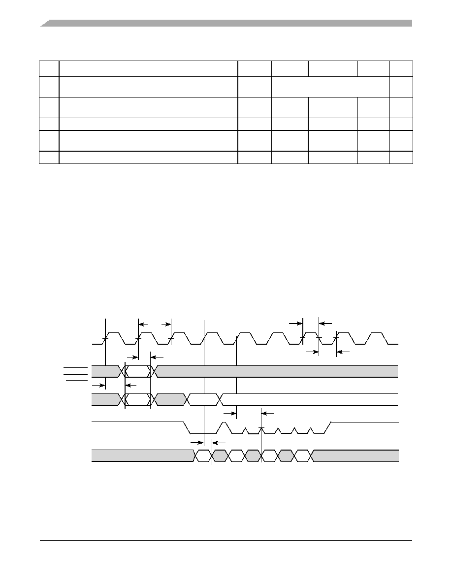
Figure 11. SDR Write Timing
SD8 SD_DQS[3:2] input hold relative to SD_CLK
tDQISDCH
Does not apply. 0.5
×SD_CLK fixed
width.
6
SD9 Data (D[31:0]) Input Setup relative to SD_CLK (reference
only)
tDVSDCH
0.25
×
SD_CLK
—ns
7
SD10 Data Input Hold relative to SD_CLK (reference only)
tDISDCH
1.0
—
ns
SD11 Data (D[31:0]) and Data Mask(SD_DQM[3:0]) Output Valid
tSDCHDMV
—0.5
× SD_CLK
+ 2
ns
SD12 Data (D[31:0]) and Data Mask (SD_DQM[3:0]) Output Hold
tSDCHDMI
1.5
—
ns
1 The device supports same frequency of operation for both FlexBus and SDRAM clock operates as that of the internal bus clock.
Please see the PLL chapter of the device reference manual for more information on setting the SDRAM clock rate.
2 SD_CLK is one SDRAM clock in ns.
3 Pulse width high plus pulse width low cannot exceed min and max clock period.
4 SD_SDR_DQS is designed to pulse 0.25 clock before the rising edge of the memory clock. This is a guideline only. Subtle
variation from this guideline is expected. SD_SDR_DQS will only pulse during a read cycle and one pulse will occur for each
data beat.
5 SD_DQS is designed to pulse 0.25 clock before the rising edge of the memory clock. This spec is a guideline only. Subtle
variation from this guideline is expected. SD_DQS will only pulse during a read cycle and one pulse will occur for each data
beat.
6 The SD_DQS pulse is designed to be 0.5 clock in width. The timing of the rising edge is most important. The falling edge does
not affect the memory controller.
7 Since a read cycle in SDR mode still uses the DQS circuit within the device, it is critical that the data valid window be centered
1/4 clk after the rising edge of DQS. Ensuring that this happens will result in successful SDR reads. The input setup spec is
provided as guidance.
Table 14. SDR Timing Specifications (continued)
Num
Characteristic
Symbol
Min
Max
Unit
Notes
SD_CLK
SDDM
D[31:0]
A[23:0]
SD_BA[1:0]
CMD
ROW
SD1
SD4
COL
SD5
WD1
WD2
WD3
WD4
SD12
SD11
SD_CSn
SD_RAS
SD_WE
SD_CAS
SD2
SD3
相关PDF资料 |
PDF描述 |
|---|---|
| MCF5251CVM140 | IC MPU 32BIT 140MHZ 225-MAPBGA |
| MCF5253CVM140J | IC MCU 2.1MIPS 140MHZ 225MAPBGA |
| MCF5270CVM150 | IC MCU 32BIT 150MHZ 196-MAPBGA |
| MCF5272VF66J | IC MCU 32BIT 66MHZ 196-MAPBGA |
| MCF5275CVM166 | IC MCU 32BIT 166MHZ 256-MAPBGA |
相关代理商/技术参数 |
参数描述 |
|---|---|
| MCF5232 | 制造商:FREESCALE 制造商全称:Freescale Semiconductor, Inc 功能描述:Integrated Microprocessor Hardware Specification |
| MCF5232160QFP | 制造商:FREESCALE 制造商全称:Freescale Semiconductor, Inc 功能描述:Integrated Microprocessor Hardware Specification |
| MCF5232196MAPBGA | 制造商:FREESCALE 制造商全称:Freescale Semiconductor, Inc 功能描述:Integrated Microprocessor Hardware Specification |
| MCF5232CAB80 | 功能描述:微处理器 - MPU MCF5232 V2CORE 64KSRAM RoHS:否 制造商:Atmel 处理器系列:SAMA5D31 核心:ARM Cortex A5 数据总线宽度:32 bit 最大时钟频率:536 MHz 程序存储器大小:32 KB 数据 RAM 大小:128 KB 接口类型:CAN, Ethernet, LIN, SPI,TWI, UART, USB 工作电源电压:1.8 V to 3.3 V 最大工作温度:+ 85 C 安装风格:SMD/SMT 封装 / 箱体:FBGA-324 |
| MCF5232CVM100 | 功能描述:微处理器 - MPU MCF5232 V2CORE 64KSRAM RoHS:否 制造商:Atmel 处理器系列:SAMA5D31 核心:ARM Cortex A5 数据总线宽度:32 bit 最大时钟频率:536 MHz 程序存储器大小:32 KB 数据 RAM 大小:128 KB 接口类型:CAN, Ethernet, LIN, SPI,TWI, UART, USB 工作电源电压:1.8 V to 3.3 V 最大工作温度:+ 85 C 安装风格:SMD/SMT 封装 / 箱体:FBGA-324 |
发布紧急采购,3分钟左右您将得到回复。