- 您现在的位置:买卖IC网 > PDF目录45311 > MCF53013CQT240 (FREESCALE SEMICONDUCTOR INC) MICROPROCESSOR, PQFP208 PDF资料下载
参数资料
| 型号: | MCF53013CQT240 |
| 厂商: | FREESCALE SEMICONDUCTOR INC |
| 元件分类: | 微控制器/微处理器 |
| 英文描述: | MICROPROCESSOR, PQFP208 |
| 封装: | 28 X 28 MM, ROHS COMPLIANT, LQFP-208 |
| 文件页数: | 21/62页 |
| 文件大小: | 2365K |
| 代理商: | MCF53013CQT240 |
第1页第2页第3页第4页第5页第6页第7页第8页第9页第10页第11页第12页第13页第14页第15页第16页第17页第18页第19页第20页当前第21页第22页第23页第24页第25页第26页第27页第28页第29页第30页第31页第32页第33页第34页第35页第36页第37页第38页第39页第40页第41页第42页第43页第44页第45页第46页第47页第48页第49页第50页第51页第52页第53页第54页第55页第56页第57页第58页第59页第60页第61页第62页
MCF5301x Data Sheet, Rev. 5
Preliminary—Subject to Change Without Notice
Preliminary Electrical Characteristics
Freescale Semiconductor
28
read cycles. Care must be taken during board design to adhere to the following guidelines and specs with regard to the
SD_SDR_DQS signal and its usage.
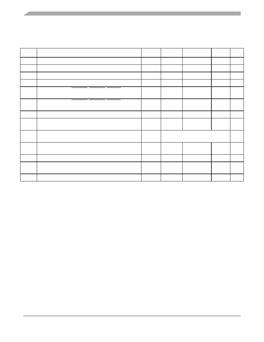
Table 13. SDR Timing Specifications
Symbol
Characteristic
Symbol
Min
Max
Unit
Notes
Frequency of operation
50
80
Mhz
1
The device supports same frequency of operation for both FlexBus and SDRAM clock operates as that of the internal bus clock.
Please see the PLL chapter of the MCF5301x Reference Manual for more information on setting the SDRAM clock rate.
SD1
Clock period
tSDCK
12.5
20
ns
2
SD_CLK is one SDRAM clock in (ns).
SD2
Pulse width high
tSDCKH
0.45
0.55
SD_CLK
3
Pulse width high plus pulse width low cannot exceed min and max clock period.
SD3
Pulse width low
tSDCKH
0.45
0.55
SD_CLK
4
Pulse width high plus pulse width low cannot exceed min and max clock period.
SD4
Address, SD_CKE, SD_CAS, SD_RAS, SD_WE, SD_BA,
SD_CS[1:0] output valid
tSDCHACV
—0.5
× SD_CLK
+1.0
ns
SD5
Address, SD_CKE, SD_CAS, SD_RAS, SD_WE, SD_BA,
SD_CS[1:0] output hold
tSDCHACI
2.0
—
ns
SD6
SD_SDR_DQS output valid
tDQSOV
—
Self timed
ns
5
SD_DQS is designed to pulse 0.25 clock before the rising edge of the memory clock. This is a guideline only. Subtle variation
from this guideline is expected. SD_DQS will only pulse during a read cycle and one pulse will occur for each data beat.
SD7
SD_DQS[3:0] input setup relative to SD_CLK
tDQVSDCH
0.25
×
SD_CLK
0.40
× SD_CLK
ns
6
SDR_DQS is designed to pulse 0.25 clock before the rising edge of the memory clock. This spec is a guideline only. Subtle
variation from this guideline is expected. SDR_DQS will only pulse during a read cycle and one pulse will occur for each data
beat.
SD8
SD_DQS[3:2] input hold relative to SD_CLK
tDQISDCH
Does not apply. 0.5
×SD_CLK fixed
width.
7
The SDR_DQS pulse is designed to be 0.5 clock in width. The timing of the rising edge is most important. The falling edge does
not affect the memory controller.
SD9
Data (D[31:0]) input setup relative to SD_CLK (reference
only)
tDVSDCH
0.25
×
SD_CLK
—ns
8
Since a read cycle in SDR mode still uses the DQS circuit within the device, it is most critical that the data valid window be
centered 1/4 clk after the rising edge of DQS. Ensuring that this happens will result in successful SDR reads. The input setup
spec is just provided as guidance.
SD10
Data input hold relative to SD_CLK (reference only)
tDISDCH
1.0
—
ns
SD11
Data (D[31:0]) and data mask (SD_DQM[3:0]) output valid
tSDCHDMV
—0.75
× SD_CLK
+ 0.5
ns
SD12
Data (D[31:0]) and data mask (SD_DQM[3:0]) output hold
tSDCHDMI
1.5
—
ns
相关PDF资料 |
PDF描述 |
|---|---|
| MCF5307CFT66B | 32-BIT, 66 MHz, RISC PROCESSOR, PQFP208 |
| MCF5307FT90BB1 | 32-BIT, 90 MHz, RISC PROCESSOR, PQFP208 |
| MCF5307AI66B | 32-BIT, 66 MHz, RISC PROCESSOR, PQFP208 |
| MCF5307FT66B | 32-BIT, 66 MHz, RISC PROCESSOR, PQFP208 |
| MCF5307FT90B | 32-BIT, 90 MHz, RISC PROCESSOR, PQFP208 |
相关代理商/技术参数 |
参数描述 |
|---|---|
| MCF53014CMJ240 | 制造商:Freescale Semiconductor 功能描述:MCF5301X RISC 32-BIT CMOS 240MHZ 3.3V - Bulk 制造商:Rochester Electronics LLC 功能描述: |
| MCF53014CMJ240J | 功能描述:32位微控制器 - MCU CFV3 RoHS:否 制造商:Texas Instruments 核心:C28x 处理器系列:TMS320F28x 数据总线宽度:32 bit 最大时钟频率:90 MHz 程序存储器大小:64 KB 数据 RAM 大小:26 KB 片上 ADC:Yes 工作电源电压:2.97 V to 3.63 V 工作温度范围:- 40 C to + 105 C 封装 / 箱体:LQFP-80 安装风格:SMD/SMT |
| MCF53015CMJ240 | 制造商:Freescale Semiconductor 功能描述:MCF5301X RISC 32-BIT CMOS 240MHZ 3.3V - Bulk |
| MCF53015CMJ240J | 功能描述:32位微控制器 - MCU CFV3 SECURITY RoHS:否 制造商:Texas Instruments 核心:C28x 处理器系列:TMS320F28x 数据总线宽度:32 bit 最大时钟频率:90 MHz 程序存储器大小:64 KB 数据 RAM 大小:26 KB 片上 ADC:Yes 工作电源电压:2.97 V to 3.63 V 工作温度范围:- 40 C to + 105 C 封装 / 箱体:LQFP-80 安装风格:SMD/SMT |
| MCF53016CMJ240 | 制造商:Freescale Semiconductor 功能描述:LONGJING C&I CFV3 VOIP - Bulk |
发布紧急采购,3分钟左右您将得到回复。