- 您现在的位置:买卖IC网 > PDF目录11963 > MCHC11F1CFNE3 (Freescale Semiconductor)IC MCU 8BIT 1K RAM 68-PLCC PDF资料下载
参数资料
| 型号: | MCHC11F1CFNE3 |
| 厂商: | Freescale Semiconductor |
| 文件页数: | 143/158页 |
| 文件大小: | 0K |
| 描述: | IC MCU 8BIT 1K RAM 68-PLCC |
| 标准包装: | 18 |
| 系列: | HC11 |
| 核心处理器: | HC11 |
| 芯体尺寸: | 8-位 |
| 速度: | 3MHz |
| 连通性: | SCI,SPI |
| 外围设备: | POR,WDT |
| 输入/输出数: | 30 |
| 程序存储器类型: | ROMless |
| EEPROM 大小: | 512 x 8 |
| RAM 容量: | 1K x 8 |
| 电压 - 电源 (Vcc/Vdd): | 4.75 V ~ 5.25 V |
| 数据转换器: | A/D 8x8b |
| 振荡器型: | 内部 |
| 工作温度: | -40°C ~ 85°C |
| 封装/外壳: | 68-LCC(J 形引线) |
| 包装: | 管件 |
第1页第2页第3页第4页第5页第6页第7页第8页第9页第10页第11页第12页第13页第14页第15页第16页第17页第18页第19页第20页第21页第22页第23页第24页第25页第26页第27页第28页第29页第30页第31页第32页第33页第34页第35页第36页第37页第38页第39页第40页第41页第42页第43页第44页第45页第46页第47页第48页第49页第50页第51页第52页第53页第54页第55页第56页第57页第58页第59页第60页第61页第62页第63页第64页第65页第66页第67页第68页第69页第70页第71页第72页第73页第74页第75页第76页第77页第78页第79页第80页第81页第82页第83页第84页第85页第86页第87页第88页第89页第90页第91页第92页第93页第94页第95页第96页第97页第98页第99页第100页第101页第102页第103页第104页第105页第106页第107页第108页第109页第110页第111页第112页第113页第114页第115页第116页第117页第118页第119页第120页第121页第122页第123页第124页第125页第126页第127页第128页第129页第130页第131页第132页第133页第134页第135页第136页第137页第138页第139页第140页第141页第142页当前第143页第144页第145页第146页第147页第148页第149页第150页第151页第152页第153页第154页第155页第156页第157页第158页
PARALLEL INPUT/OUTPUT
TECHNICAL DATA
6-5
6.7 Port G
Port G pins reset to high-impedance inputs except in expanded modes where reset
causes PG7 to become the CSPROG output. Alternate functions for port G bits [7:4]
are chip select outputs. All port G bits are bidirectional and have corresponding data
direction bits.
The GWOM control bit in the OPT2 register disables port G's P-channel output drivers.
Because the N-channel driver is not affected by GWOM, setting GWOM causes port
G to become an open-drain-type output port suitable for wired-OR operation. In wired-
OR mode, (PORTG bits are at logic level zero), pins are actively driven low by the N-
channel driver. When a port G bit is at logic level one, the associated pin is in a high-
impedance state, as neither the N-channel nor the P-channel devices are active. It is
customary to have an external pull-up resistor on lines that are driven by open-drain
devices. Port G can be configured for wired-OR operation in any operating mode.
DDG[7:0] — Data Direction for Port G
0 = Input
1 = Output
6.8 System Configuration Options 2
The system configuration options 2 register controls several configuration parameters.
Bit 6, CWOM, is the only bit in this register that directly affects parallel I/O.
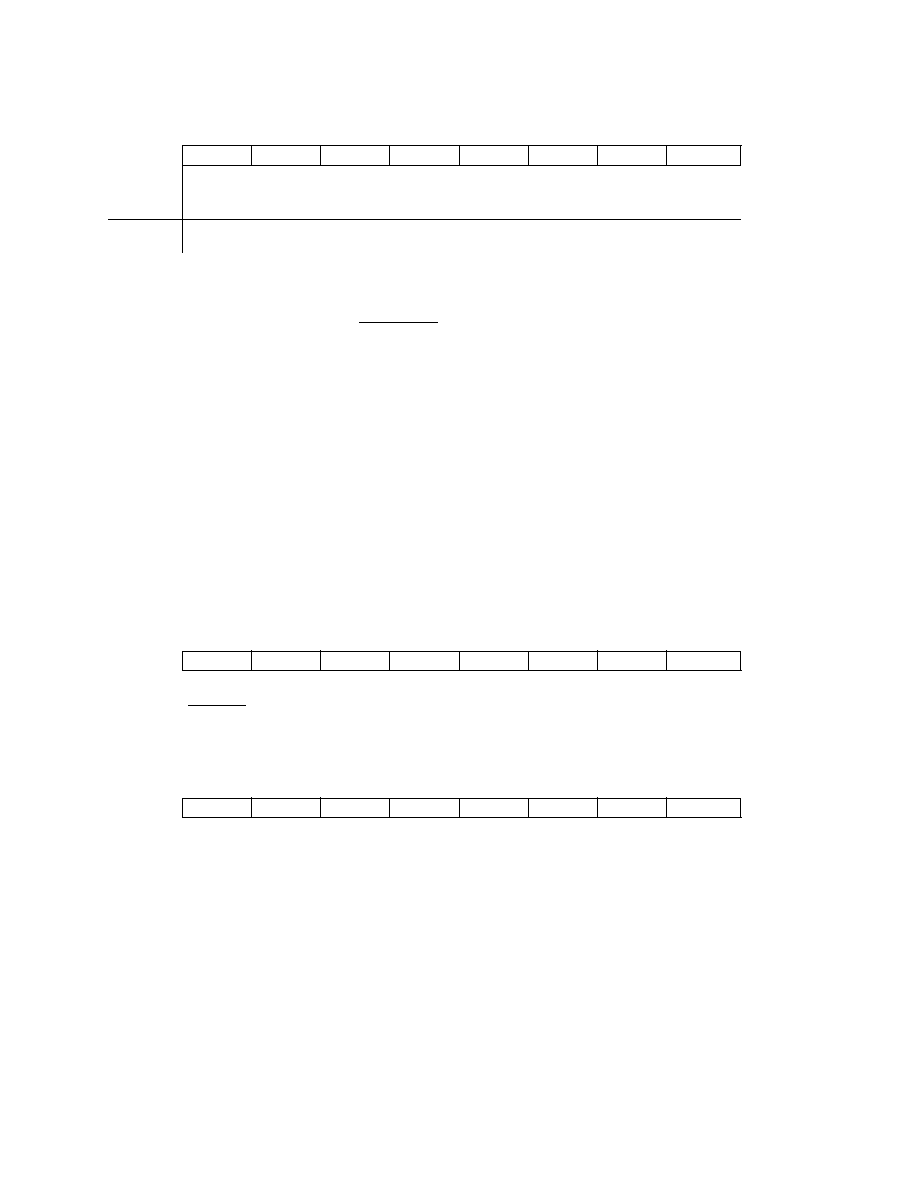
PORTF — Port F Data
$1005
Bit 7
654321
Bit 0
PF7
PF6
PF5
PF4
PF3
PF2
PF1
PF0
S. Chip
or Boot:
PF7
PF6
PF5
PF4
PF3
PF2
PF1
PF0
RESET:
0000000
0
Expan.
or Test:
ADDR7
ADDR6
ADDR5
ADDR4
ADDR3
ADDR2
ADDR1
ADDR0
PORTG — Port G Data
$1002
Bit 7
654321
Bit 0
PG7
PG6
PG5
PG4
PG3
PG2
PG1
PG0
RESET:
IIIIIII
I
Alt. Pin
Func.: CSPROG
CSGEN
CSIO1
CSIO2
—
DDRG — Data Direction Register for Port G
$1003
Bit 7
654321
Bit 0
DDG7
DDG6
DDG5
DDG4
DDG3
DDG2
DDG1
DDG0
RESET:
0000000
0
F
re
e
sc
a
le
S
e
m
ic
o
n
d
u
c
to
r,
I
Freescale Semiconductor, Inc.
For More Information On This Product,
Go to: www.freescale.com
n
c
..
.
相关PDF资料 |
PDF描述 |
|---|---|
| VJ2225A153KBBAT4X | CAP CER 0.015UF 100V NP0 2225 |
| VE-B6V-IY-F1 | CONVERTER MOD DC/DC 5.8V 50W |
| VJ2225A153KBCAT4X | CAP CER 0.015UF 200V NP0 2225 |
| VE-B6D-IY-F3 | CONVERTER MOD DC/DC 85V 50W |
| VE-B6D-IY-F1 | CONVERTER MOD DC/DC 85V 50W |
相关代理商/技术参数 |
参数描述 |
|---|---|
| MCHC11F1CFNE3 | 制造商:Freescale Semiconductor 功能描述:8-Bit Microcontroller IC |
| MCHC11F1CFNE3R | 功能描述:8位微控制器 -MCU 8B MCU 1KRAM 512EE RoHS:否 制造商:Silicon Labs 核心:8051 处理器系列:C8051F39x 数据总线宽度:8 bit 最大时钟频率:50 MHz 程序存储器大小:16 KB 数据 RAM 大小:1 KB 片上 ADC:Yes 工作电源电压:1.8 V to 3.6 V 工作温度范围:- 40 C to + 105 C 封装 / 箱体:QFN-20 安装风格:SMD/SMT |
| MCHC11F1CFNE4 | 功能描述:8位微控制器 -MCU 8B MCU 1KRAM 512EE RoHS:否 制造商:Silicon Labs 核心:8051 处理器系列:C8051F39x 数据总线宽度:8 bit 最大时钟频率:50 MHz 程序存储器大小:16 KB 数据 RAM 大小:1 KB 片上 ADC:Yes 工作电源电压:1.8 V to 3.6 V 工作温度范围:- 40 C to + 105 C 封装 / 箱体:QFN-20 安装风格:SMD/SMT |
| MCHC11F1CFNE4R | 功能描述:8位微控制器 -MCU 8B MCU 1KRAM 512EE RoHS:否 制造商:Silicon Labs 核心:8051 处理器系列:C8051F39x 数据总线宽度:8 bit 最大时钟频率:50 MHz 程序存储器大小:16 KB 数据 RAM 大小:1 KB 片上 ADC:Yes 工作电源电压:1.8 V to 3.6 V 工作温度范围:- 40 C to + 105 C 封装 / 箱体:QFN-20 安装风格:SMD/SMT |
| MCHC11F1CFNE5 | 功能描述:8位微控制器 -MCU 8B MCU 1KRAM 512EE RoHS:否 制造商:Silicon Labs 核心:8051 处理器系列:C8051F39x 数据总线宽度:8 bit 最大时钟频率:50 MHz 程序存储器大小:16 KB 数据 RAM 大小:1 KB 片上 ADC:Yes 工作电源电压:1.8 V to 3.6 V 工作温度范围:- 40 C to + 105 C 封装 / 箱体:QFN-20 安装风格:SMD/SMT |
发布紧急采购,3分钟左右您将得到回复。