- 您现在的位置:买卖IC网 > PDF目录11963 > MCHC11F1CFNE3 (Freescale Semiconductor)IC MCU 8BIT 1K RAM 68-PLCC PDF资料下载
参数资料
| 型号: | MCHC11F1CFNE3 |
| 厂商: | Freescale Semiconductor |
| 文件页数: | 73/158页 |
| 文件大小: | 0K |
| 描述: | IC MCU 8BIT 1K RAM 68-PLCC |
| 标准包装: | 18 |
| 系列: | HC11 |
| 核心处理器: | HC11 |
| 芯体尺寸: | 8-位 |
| 速度: | 3MHz |
| 连通性: | SCI,SPI |
| 外围设备: | POR,WDT |
| 输入/输出数: | 30 |
| 程序存储器类型: | ROMless |
| EEPROM 大小: | 512 x 8 |
| RAM 容量: | 1K x 8 |
| 电压 - 电源 (Vcc/Vdd): | 4.75 V ~ 5.25 V |
| 数据转换器: | A/D 8x8b |
| 振荡器型: | 内部 |
| 工作温度: | -40°C ~ 85°C |
| 封装/外壳: | 68-LCC(J 形引线) |
| 包装: | 管件 |
第1页第2页第3页第4页第5页第6页第7页第8页第9页第10页第11页第12页第13页第14页第15页第16页第17页第18页第19页第20页第21页第22页第23页第24页第25页第26页第27页第28页第29页第30页第31页第32页第33页第34页第35页第36页第37页第38页第39页第40页第41页第42页第43页第44页第45页第46页第47页第48页第49页第50页第51页第52页第53页第54页第55页第56页第57页第58页第59页第60页第61页第62页第63页第64页第65页第66页第67页第68页第69页第70页第71页第72页当前第73页第74页第75页第76页第77页第78页第79页第80页第81页第82页第83页第84页第85页第86页第87页第88页第89页第90页第91页第92页第93页第94页第95页第96页第97页第98页第99页第100页第101页第102页第103页第104页第105页第106页第107页第108页第109页第110页第111页第112页第113页第114页第115页第116页第117页第118页第119页第120页第121页第122页第123页第124页第125页第126页第127页第128页第129页第130页第131页第132页第133页第134页第135页第136页第137页第138页第139页第140页第141页第142页第143页第144页第145页第146页第147页第148页第149页第150页第151页第152页第153页第154页第155页第156页第157页第158页
PIN DESCRIPTIONS
TECHNICAL DATA
2-7
2.11.1 Port A
Port A is an 8-bit general-purpose I/O port with a data register (PORTA) and a data
direction register (DDRA). Port A pins share functions with the 16-bit timer system.
PORTA can be read at any time. Inputs return the pin level; outputs return the pin driv-
er input level. If written, PORTA stores the data in internal latches. It drives the pins
only if they are configured as outputs. Writes to PORTA do not change the pin state
when the pins are configured for timer output compares.
Out of reset, port A pins [7:0] are general-purpose high-impedance inputs. When the
timer functions associated with these pins are disabled, the bits in DDRA govern the
I/O state of the associated pin. For further information, refer to SECTION 6 PARAL-
NOTE
When using the information about port functions, do not confuse pin
function with the electrical state of the pin at reset. All general-pur-
pose I/O pins configured as inputs at reset are in a high-impedance
state. Port data registers reflect the logic state of the port at reset.
The pin function is mode dependent.
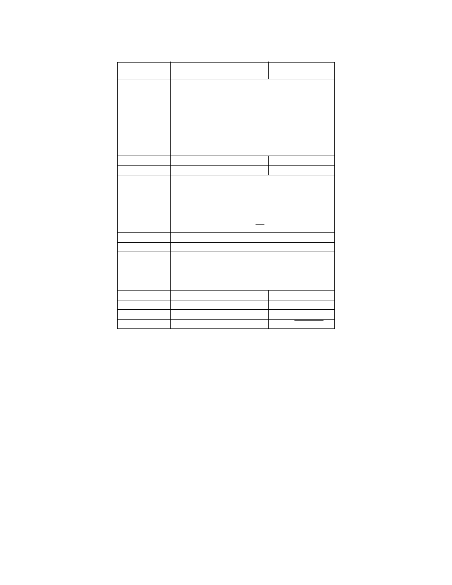
Table 2-1 Port Signal Functions
Port/Bit
Single-Chip and
Bootstrap Mode
Expanded and
Special Test Mode
PA0
PA0/IC3
PA1
PA1/IC2
PA2
PA2/IC1
PA3
PA3/OC5/IC4/OC1
PA4
PA4/OC4/OC1
PA5
PA5/OC3/OC1
PA6
PA6/OC2/OC1
PA7
PA7/PAI/OC1
PB[7:0]
ADDR[15:8]
PC[7:0]
DATA[7:0]
PD0
PD0/RxD
PD1
PD1/TxD
PD2
PD2/MISO
PD3
PD3/MOSI
PD4
PD4/SCK
PD5
PD5/SS
PE[7:0]
PE[7:0]/AN[7:0]
PF[7:0]
ADDR[7:0]
PG0
PG1
PG2
PG3
PG4
PG4/CSIO2
PG5
PG5/CSIO1
PG6
PG6/CSGEN
PG7
PG7/CSPROG
F
re
e
sc
a
le
S
e
m
ic
o
n
d
u
c
to
r,
I
Freescale Semiconductor, Inc.
For More Information On This Product,
Go to: www.freescale.com
n
c
..
.
相关PDF资料 |
PDF描述 |
|---|---|
| VJ2225A153KBBAT4X | CAP CER 0.015UF 100V NP0 2225 |
| VE-B6V-IY-F1 | CONVERTER MOD DC/DC 5.8V 50W |
| VJ2225A153KBCAT4X | CAP CER 0.015UF 200V NP0 2225 |
| VE-B6D-IY-F3 | CONVERTER MOD DC/DC 85V 50W |
| VE-B6D-IY-F1 | CONVERTER MOD DC/DC 85V 50W |
相关代理商/技术参数 |
参数描述 |
|---|---|
| MCHC11F1CFNE3 | 制造商:Freescale Semiconductor 功能描述:8-Bit Microcontroller IC |
| MCHC11F1CFNE3R | 功能描述:8位微控制器 -MCU 8B MCU 1KRAM 512EE RoHS:否 制造商:Silicon Labs 核心:8051 处理器系列:C8051F39x 数据总线宽度:8 bit 最大时钟频率:50 MHz 程序存储器大小:16 KB 数据 RAM 大小:1 KB 片上 ADC:Yes 工作电源电压:1.8 V to 3.6 V 工作温度范围:- 40 C to + 105 C 封装 / 箱体:QFN-20 安装风格:SMD/SMT |
| MCHC11F1CFNE4 | 功能描述:8位微控制器 -MCU 8B MCU 1KRAM 512EE RoHS:否 制造商:Silicon Labs 核心:8051 处理器系列:C8051F39x 数据总线宽度:8 bit 最大时钟频率:50 MHz 程序存储器大小:16 KB 数据 RAM 大小:1 KB 片上 ADC:Yes 工作电源电压:1.8 V to 3.6 V 工作温度范围:- 40 C to + 105 C 封装 / 箱体:QFN-20 安装风格:SMD/SMT |
| MCHC11F1CFNE4R | 功能描述:8位微控制器 -MCU 8B MCU 1KRAM 512EE RoHS:否 制造商:Silicon Labs 核心:8051 处理器系列:C8051F39x 数据总线宽度:8 bit 最大时钟频率:50 MHz 程序存储器大小:16 KB 数据 RAM 大小:1 KB 片上 ADC:Yes 工作电源电压:1.8 V to 3.6 V 工作温度范围:- 40 C to + 105 C 封装 / 箱体:QFN-20 安装风格:SMD/SMT |
| MCHC11F1CFNE5 | 功能描述:8位微控制器 -MCU 8B MCU 1KRAM 512EE RoHS:否 制造商:Silicon Labs 核心:8051 处理器系列:C8051F39x 数据总线宽度:8 bit 最大时钟频率:50 MHz 程序存储器大小:16 KB 数据 RAM 大小:1 KB 片上 ADC:Yes 工作电源电压:1.8 V to 3.6 V 工作温度范围:- 40 C to + 105 C 封装 / 箱体:QFN-20 安装风格:SMD/SMT |
发布紧急采购,3分钟左右您将得到回复。