- 您现在的位置:买卖IC网 > PDF目录10940 > MCIMX27LVOP4A (Freescale Semiconductor)IC LOW END I.MX27 404-MAPBGA PDF资料下载
参数资料
| 型号: | MCIMX27LVOP4A |
| 厂商: | Freescale Semiconductor |
| 文件页数: | 138/152页 |
| 文件大小: | 0K |
| 描述: | IC LOW END I.MX27 404-MAPBGA |
| 视频文件: | i.MX27 Multimedia Application Processor |
| 标准包装: | 90 |
| 系列: | i.MX27 |
| 核心处理器: | ARM9 |
| 芯体尺寸: | 32-位 |
| 速度: | 400MHz |
| 连通性: | 1 线,CAN,EBI/EMI,以太网,I²C,MMC,智能卡,SPI,SSI,UART/USART,USB OTG |
| 外围设备: | DMA,LCD,POR,PWM,WDT |
| 程序存储器类型: | ROMless |
| RAM 容量: | 45K x 8 |
| 电压 - 电源 (Vcc/Vdd): | 1.38 V ~ 1.52 V |
| 振荡器型: | 外部 |
| 工作温度: | -20°C ~ 85°C |
| 封装/外壳: | 404-LFBGA |
| 包装: | 托盘 |
第1页第2页第3页第4页第5页第6页第7页第8页第9页第10页第11页第12页第13页第14页第15页第16页第17页第18页第19页第20页第21页第22页第23页第24页第25页第26页第27页第28页第29页第30页第31页第32页第33页第34页第35页第36页第37页第38页第39页第40页第41页第42页第43页第44页第45页第46页第47页第48页第49页第50页第51页第52页第53页第54页第55页第56页第57页第58页第59页第60页第61页第62页第63页第64页第65页第66页第67页第68页第69页第70页第71页第72页第73页第74页第75页第76页第77页第78页第79页第80页第81页第82页第83页第84页第85页第86页第87页第88页第89页第90页第91页第92页第93页第94页第95页第96页第97页第98页第99页第100页第101页第102页第103页第104页第105页第106页第107页第108页第109页第110页第111页第112页第113页第114页第115页第116页第117页第118页第119页第120页第121页第122页第123页第124页第125页第126页第127页第128页第129页第130页第131页第132页第133页第134页第135页第136页第137页当前第138页第139页第140页第141页第142页第143页第144页第145页第146页第147页第148页第149页第150页第151页第152页
i.MX27 and i.MX27L Data Sheet, Rev. 1.8
86
Freescale Semiconductor
Electrical Characteristics
All the timings for the SSI are given for a non-inverted serial clock polarity (TSCKP/RSCKP = 0)
and a non-inverted frame sync (TFSI/RFSI = 0). If the polarity of the clock and/or the frame sync
have been inverted, all the timing remains valid by inverting the clock signal STCK/SRCK and/or
the frame sync STFS/SRFS shown in the tables and in the figures.
All timings are on AUDMUX pads when SSI is being used for data transfer.
“Tx” and “Rx” refer to the Transmit and Receive sections of the SSI.
For internal Frame Sync operation using external clock, the FS timing will be same as that of Tx
Data (for example, during AC97 mode of operation).
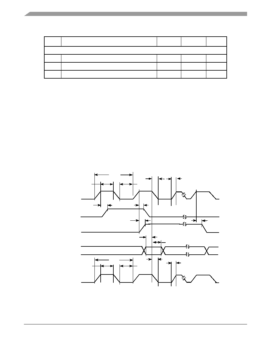
4.3.11.2
SSI Receiver Timing with Internal Clock
Figure 47 and Figure 48 show the SSI receiver timing with internal clock, and Table 47 lists the timing
parameters.
Figure 47. SSI Receiver with Internal Clock Timing Diagram
Synchronous Internal Clock Operation
SS42
SRXD setup before (Tx) CK falling
10.0
—
ns
SS43
SRXD hold after (Tx) CK falling
0
—
ns
SS52
Loading
—
25
pF
Table 46. SSI Transmitter with Internal Clock Timing Parameters (continued)
ID
Parameter
Min
Max
Unit
SS50
SS48
AD1_TXC
AD1_TXFS (bl)
AD1_TXFS (wl)
AD1_RXD
AD1_RXC
SS1
SS4
SS2
SS51
SS20
SS21
SS49
SS7
SS9
SS11
SS13
SS47
(Output)
(Input)
(Output)
SS3
SS5
相关PDF资料 |
PDF描述 |
|---|---|
| MCIMX27LMOP4A | IC MPU I.MX27 IN 19X19 473MAPBGA |
| MCIMX31LDVMN5DR2 | IC MPU I.MX31L CONSUMR 473MAPBGA |
| 302S43W151KV4E | CAP CER 150PF 3KV 10% X7R 1812 |
| JBXER0G05FSSDSR | CONN RCPT 5POS FRONT PNL MNT SLD |
| MCIMX31LDVKN5DR2 | IC MPU I/MX31L CONSUMR 457MAPBGA |
相关代理商/技术参数 |
参数描述 |
|---|---|
| MCIMX27LVOP4AR2 | 功能描述:处理器 - 专门应用 LOW END I.MX27 RoHS:否 制造商:Freescale Semiconductor 类型:Multimedia Applications 核心:ARM Cortex A9 处理器系列:i.MX6 数据总线宽度:32 bit 最大时钟频率:1 GHz 指令/数据缓存: 数据 RAM 大小:128 KB 数据 ROM 大小: 工作电源电压: 最大工作温度:+ 95 C 安装风格:SMD/SMT 封装 / 箱体:MAPBGA-432 |
| MCIMX27MJP4A | 功能描述:处理器 - 专门应用 Multimedia App Processor RoHS:否 制造商:Freescale Semiconductor 类型:Multimedia Applications 核心:ARM Cortex A9 处理器系列:i.MX6 数据总线宽度:32 bit 最大时钟频率:1 GHz 指令/数据缓存: 数据 RAM 大小:128 KB 数据 ROM 大小: 工作电源电压: 最大工作温度:+ 95 C 安装风格:SMD/SMT 封装 / 箱体:MAPBGA-432 |
| MCIMX27MJP4AR2 | 功能描述:处理器 - 专门应用 Bono 19x19 FG RoHS:否 制造商:Freescale Semiconductor 类型:Multimedia Applications 核心:ARM Cortex A9 处理器系列:i.MX6 数据总线宽度:32 bit 最大时钟频率:1 GHz 指令/数据缓存: 数据 RAM 大小:128 KB 数据 ROM 大小: 工作电源电压: 最大工作温度:+ 95 C 安装风格:SMD/SMT 封装 / 箱体:MAPBGA-432 |
| MCIMX27MOP4A | 功能描述:处理器 - 专门应用 BONO 19X19 FG RoHS:否 制造商:Freescale Semiconductor 类型:Multimedia Applications 核心:ARM Cortex A9 处理器系列:i.MX6 数据总线宽度:32 bit 最大时钟频率:1 GHz 指令/数据缓存: 数据 RAM 大小:128 KB 数据 ROM 大小: 工作电源电压: 最大工作温度:+ 95 C 安装风格:SMD/SMT 封装 / 箱体:MAPBGA-432 |
| MCIMX27MOP4AR2 | 功能描述:处理器 - 专门应用 BONO 19X19 R2 RoHS:否 制造商:Freescale Semiconductor 类型:Multimedia Applications 核心:ARM Cortex A9 处理器系列:i.MX6 数据总线宽度:32 bit 最大时钟频率:1 GHz 指令/数据缓存: 数据 RAM 大小:128 KB 数据 ROM 大小: 工作电源电压: 最大工作温度:+ 95 C 安装风格:SMD/SMT 封装 / 箱体:MAPBGA-432 |
发布紧急采购,3分钟左右您将得到回复。