- 您现在的位置:买卖IC网 > PDF目录80477 > MCIMX31CJMN4C (FREESCALE SEMICONDUCTOR INC) 32-BIT, 400 MHz, MICROPROCESSOR, PBGA473 PDF资料下载
参数资料
| 型号: | MCIMX31CJMN4C |
| 厂商: | FREESCALE SEMICONDUCTOR INC |
| 元件分类: | 微控制器/微处理器 |
| 英文描述: | 32-BIT, 400 MHz, MICROPROCESSOR, PBGA473 |
| 封装: | 19 X 19 MM, 0.80 MM PITCH, ROHS COMPLIANT, PLASTIC, BGA-473 |
| 文件页数: | 79/108页 |
| 文件大小: | 2878K |
| 代理商: | MCIMX31CJMN4C |
第1页第2页第3页第4页第5页第6页第7页第8页第9页第10页第11页第12页第13页第14页第15页第16页第17页第18页第19页第20页第21页第22页第23页第24页第25页第26页第27页第28页第29页第30页第31页第32页第33页第34页第35页第36页第37页第38页第39页第40页第41页第42页第43页第44页第45页第46页第47页第48页第49页第50页第51页第52页第53页第54页第55页第56页第57页第58页第59页第60页第61页第62页第63页第64页第65页第66页第67页第68页第69页第70页第71页第72页第73页第74页第75页第76页第77页第78页当前第79页第80页第81页第82页第83页第84页第85页第86页第87页第88页第89页第90页第91页第92页第93页第94页第95页第96页第97页第98页第99页第100页第101页第102页第103页第104页第105页第106页第107页第108页
MCIMX31C/MCIMX31LC Technical Data, Rev. 4.3
72
Freescale Semiconductor
Electrical Characteristics
The DISP#_IF_CLK_PER_WR, DISP#_IF_CLK_PER_RD, HSP_CLK_PERIOD,
DISP#_IF_CLK_DOWN_WR, DISP#_IF_CLK_UP_WR, DISP#_IF_CLK_DOWN_RD,
DISP#_IF_CLK_UP_RD and DISP#_READ_EN parameters are programmed via the
DI_DISP#_TIME_CONF_1, DI_DISP#_TIME_CONF_2 and DI_HSP_CLK_PER Registers.
4.3.15.5.3
Serial Interfaces, Functional Description
The IPU supports the following types of asynchronous serial interfaces:
3-wire (with bidirectional data line)
4-wire (with separate data input and output lines)
5-wire type 1 (with sampling RS by the serial clock)
5-wire type 2 (with sampling RS by the chip select signal)
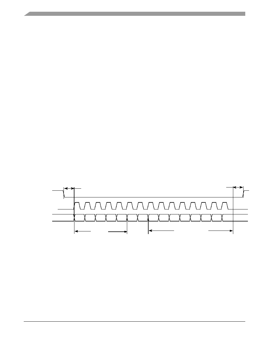
Figure 60 depicts timing of the 3-wire serial interface. The timing images correspond to active-low
DISPB_D#_CS signal and the straight polarity of the DISPB_SD_D_CLK signal.
For this interface, a bidirectional data line is used outside the device. The IPU still uses separate input and
output data lines (IPP_IND_DISPB_SD_D and IPP_DO_DISPB_SD_D). The I/O mux should provide
joining the internal data lines to the bidirectional external line according to the IPP_OBE_DISPB_SD_D
signal provided by the IPU.
Each data transfer can be preceded by an optional preamble with programmable length and contents. The
preamble is followed by read/write (RW) and address (RS) bits. The order of the these bits is
programmable. The RW bit can be disabled. The following data can consist of one word or of a whole
burst. The interface parameters are controlled by the DI_SER_DISP1_CONF and DI_SER_DISP2_CONF
Registers.
Figure 60. 3-Wire Serial Interface Timing Diagram
Figure 61 depicts timing of the 4-wire serial interface. For this interface, there are separate input and output
data lines both inside and outside the device.
Preamble
DISPB_D#_CS
DISPB_SD_D_CLK
DISPB_SD_D
RW
RS
Input or output data
D7
D6
D5
D4
D3
D2
D1
D0
1 display IF
clock cycle
1 display IF
clock cycle
Because
of
an
order
from
the
United
States
International
Trade
Commission,
BGA-packaged
product
lines
and
part
numbers
indicated
here
currently
are
not
available
from
Freescale
for
import
or
sale
in
the
United
States
prior
to
September
2010:
MCIMX31CVMN4D,
MCIMX31LCVMN4D,
MCIMX31CVMN4C,
MCIMX31LCVMN4C
相关PDF资料 |
PDF描述 |
|---|---|
| MCF52232CAF50 | 32-BIT, FLASH, 50 MHz, RISC MICROCONTROLLER, PQFP80 |
| ML9044A-XXBCVWA | 17 X 120 DOTS DOT MAT LCD DRVR AND DSPL CTLR, UUC175 |
| MC9S12XF128J0CLM | MICROCONTROLLER, PQFP112 |
| MC9S12XF512J0CLH | MICROCONTROLLER, QFP64 |
| MPC5561MVZ112R | MICROCONTROLLER, PBGA324 |
相关代理商/技术参数 |
参数描述 |
|---|---|
| MCIMX31CJMN4C | 制造商:Freescale Semiconductor 功能描述:IC 32BIT MPU 400MHZ MAPBGA-473 |
| MCIMX31CJMN4CR2 | 功能描述:处理器 - 专门应用 TORTOLA MX31 AUTO FULL RoHS:否 制造商:Freescale Semiconductor 类型:Multimedia Applications 核心:ARM Cortex A9 处理器系列:i.MX6 数据总线宽度:32 bit 最大时钟频率:1 GHz 指令/数据缓存: 数据 RAM 大小:128 KB 数据 ROM 大小: 工作电源电压: 最大工作温度:+ 95 C 安装风格:SMD/SMT 封装 / 箱体:MAPBGA-432 |
| MCIMX31CJMN4D | 功能描述:处理器 - 专门应用 MX31 2.0.1 AUTO FULL RoHS:否 制造商:Freescale Semiconductor 类型:Multimedia Applications 核心:ARM Cortex A9 处理器系列:i.MX6 数据总线宽度:32 bit 最大时钟频率:1 GHz 指令/数据缓存: 数据 RAM 大小:128 KB 数据 ROM 大小: 工作电源电压: 最大工作温度:+ 95 C 安装风格:SMD/SMT 封装 / 箱体:MAPBGA-432 |
| MCIMX31CJMN4DR2 | 功能描述:处理器 - 专门应用 MX31 2.0.1 AUTO FULL RoHS:否 制造商:Freescale Semiconductor 类型:Multimedia Applications 核心:ARM Cortex A9 处理器系列:i.MX6 数据总线宽度:32 bit 最大时钟频率:1 GHz 指令/数据缓存: 数据 RAM 大小:128 KB 数据 ROM 大小: 工作电源电压: 最大工作温度:+ 95 C 安装风格:SMD/SMT 封装 / 箱体:MAPBGA-432 |
| MCIMX31CVKN5C | 功能描述:IC MPU MAP I.MX31 457-MAPBGA RoHS:是 类别:集成电路 (IC) >> 嵌入式 - 微控制器, 系列:i.MX31 标准包装:1 系列:AVR® ATmega 核心处理器:AVR 芯体尺寸:8-位 速度:16MHz 连通性:I²C,SPI,UART/USART 外围设备:欠压检测/复位,POR,PWM,WDT 输入/输出数:32 程序存储器容量:32KB(16K x 16) 程序存储器类型:闪存 EEPROM 大小:1K x 8 RAM 容量:2K x 8 电压 - 电源 (Vcc/Vdd):2.7 V ~ 5.5 V 数据转换器:A/D 8x10b 振荡器型:内部 工作温度:-40°C ~ 125°C 封装/外壳:44-TQFP 包装:剪切带 (CT) 其它名称:ATMEGA324P-B15AZCT |
发布紧急采购,3分钟左右您将得到回复。