- 您现在的位置:买卖IC网 > PDF目录80477 > MCIMX31CJMN4C (FREESCALE SEMICONDUCTOR INC) 32-BIT, 400 MHz, MICROPROCESSOR, PBGA473 PDF资料下载
参数资料
| 型号: | MCIMX31CJMN4C |
| 厂商: | FREESCALE SEMICONDUCTOR INC |
| 元件分类: | 微控制器/微处理器 |
| 英文描述: | 32-BIT, 400 MHz, MICROPROCESSOR, PBGA473 |
| 封装: | 19 X 19 MM, 0.80 MM PITCH, ROHS COMPLIANT, PLASTIC, BGA-473 |
| 文件页数: | 93/108页 |
| 文件大小: | 2878K |
| 代理商: | MCIMX31CJMN4C |
第1页第2页第3页第4页第5页第6页第7页第8页第9页第10页第11页第12页第13页第14页第15页第16页第17页第18页第19页第20页第21页第22页第23页第24页第25页第26页第27页第28页第29页第30页第31页第32页第33页第34页第35页第36页第37页第38页第39页第40页第41页第42页第43页第44页第45页第46页第47页第48页第49页第50页第51页第52页第53页第54页第55页第56页第57页第58页第59页第60页第61页第62页第63页第64页第65页第66页第67页第68页第69页第70页第71页第72页第73页第74页第75页第76页第77页第78页第79页第80页第81页第82页第83页第84页第85页第86页第87页第88页第89页第90页第91页第92页当前第93页第94页第95页第96页第97页第98页第99页第100页第101页第102页第103页第104页第105页第106页第107页第108页
Electrical Characteristics
MCIMX31C/MCIMX31LC Technical Data, Rev. 4.3
Freescale Semiconductor
85
The interface is meant to be used with synchronous SIM cards. This means that the SIM module provides
a clock for the SIM card to use. The frequency of this clock is normally 372 times the data rate on the
TX/RX pins, however SIM module can work with CLK equal to 16 times the data rate on TX/RX pins.
There is no timing relationship between the clock and the data. The clock that the SIM module provides
to the aim card will be used by the SIM card to recover the clock from the data much like a standard UART.
All six (or 5 in case bi directional TXRX is used) of the pins for each half of the SIM module are
asynchronous to each other.
There are no required timing relationships between the signals in normal mode, but there are some in two
specific cases: reset and power down sequences.
4.3.20.1
General Timing Requirements
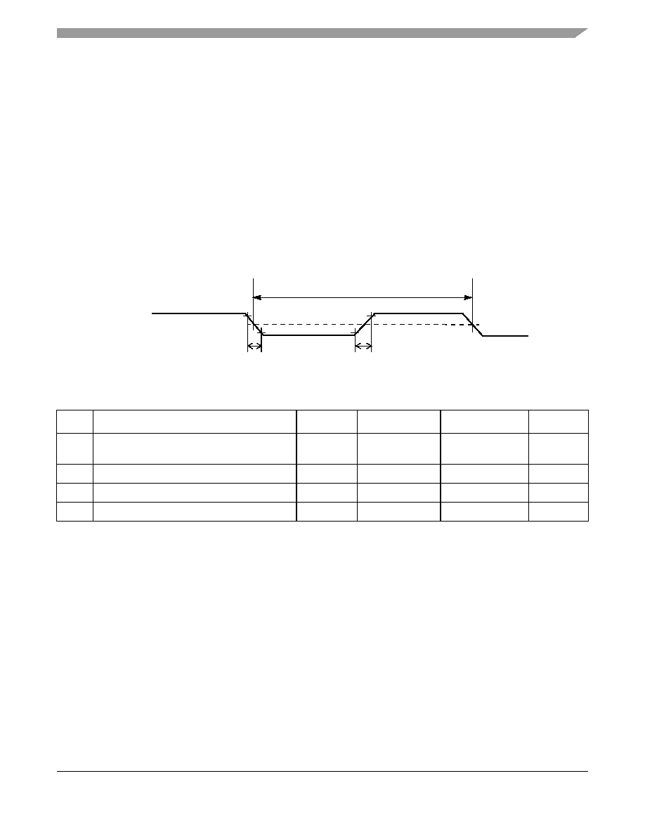
Figure 72. SIM Clock Timing Diagram
4.3.20.2
Reset Sequence
4.3.20.2.1
Cards with Internal Reset
The sequence of reset for this kind of SIM Cards is as follows (see Figure 73):
After powerup, the clock signal is enabled on SGCLK (time T0)
After 200 clock cycles, RX must be high.
The card must send a response on RX acknowledging the reset between 400 and 40000 clock
cycles after T0.
Table 54. SIM Timing Specification—High Drive Strength
Num
Description
Symbol
Min
Max
Unit
1
SIM Clock Frequency (CLK)1
1 50% duty cycle clock
Sfreq
0.01
5 (Some new cards
may reach 10)
MHz
2
SIM CLK Rise Time 2
2 With C = 50pF
Srise
—20
ns
3
SIM CLK Fall Time 3
3 With C = 50pF
Sfall
—20
ns
4
SIM Input Transition Time (RX, SIMPD)
Strans
—25
ns
CLK
Srise
Sfall
1/Sfreq
Because
of
an
order
from
the
United
States
International
Trade
Commission,
BGA-packaged
product
lines
and
part
numbers
indicated
here
currently
are
not
available
from
Freescale
for
import
or
sale
in
the
United
States
prior
to
September
2010:
MCIMX31CVMN4D,
MCIMX31LCVMN4D,
MCIMX31CVMN4C,
MCIMX31LCVMN4C
相关PDF资料 |
PDF描述 |
|---|---|
| MCF52232CAF50 | 32-BIT, FLASH, 50 MHz, RISC MICROCONTROLLER, PQFP80 |
| ML9044A-XXBCVWA | 17 X 120 DOTS DOT MAT LCD DRVR AND DSPL CTLR, UUC175 |
| MC9S12XF128J0CLM | MICROCONTROLLER, PQFP112 |
| MC9S12XF512J0CLH | MICROCONTROLLER, QFP64 |
| MPC5561MVZ112R | MICROCONTROLLER, PBGA324 |
相关代理商/技术参数 |
参数描述 |
|---|---|
| MCIMX31CJMN4C | 制造商:Freescale Semiconductor 功能描述:IC 32BIT MPU 400MHZ MAPBGA-473 |
| MCIMX31CJMN4CR2 | 功能描述:处理器 - 专门应用 TORTOLA MX31 AUTO FULL RoHS:否 制造商:Freescale Semiconductor 类型:Multimedia Applications 核心:ARM Cortex A9 处理器系列:i.MX6 数据总线宽度:32 bit 最大时钟频率:1 GHz 指令/数据缓存: 数据 RAM 大小:128 KB 数据 ROM 大小: 工作电源电压: 最大工作温度:+ 95 C 安装风格:SMD/SMT 封装 / 箱体:MAPBGA-432 |
| MCIMX31CJMN4D | 功能描述:处理器 - 专门应用 MX31 2.0.1 AUTO FULL RoHS:否 制造商:Freescale Semiconductor 类型:Multimedia Applications 核心:ARM Cortex A9 处理器系列:i.MX6 数据总线宽度:32 bit 最大时钟频率:1 GHz 指令/数据缓存: 数据 RAM 大小:128 KB 数据 ROM 大小: 工作电源电压: 最大工作温度:+ 95 C 安装风格:SMD/SMT 封装 / 箱体:MAPBGA-432 |
| MCIMX31CJMN4DR2 | 功能描述:处理器 - 专门应用 MX31 2.0.1 AUTO FULL RoHS:否 制造商:Freescale Semiconductor 类型:Multimedia Applications 核心:ARM Cortex A9 处理器系列:i.MX6 数据总线宽度:32 bit 最大时钟频率:1 GHz 指令/数据缓存: 数据 RAM 大小:128 KB 数据 ROM 大小: 工作电源电压: 最大工作温度:+ 95 C 安装风格:SMD/SMT 封装 / 箱体:MAPBGA-432 |
| MCIMX31CVKN5C | 功能描述:IC MPU MAP I.MX31 457-MAPBGA RoHS:是 类别:集成电路 (IC) >> 嵌入式 - 微控制器, 系列:i.MX31 标准包装:1 系列:AVR® ATmega 核心处理器:AVR 芯体尺寸:8-位 速度:16MHz 连通性:I²C,SPI,UART/USART 外围设备:欠压检测/复位,POR,PWM,WDT 输入/输出数:32 程序存储器容量:32KB(16K x 16) 程序存储器类型:闪存 EEPROM 大小:1K x 8 RAM 容量:2K x 8 电压 - 电源 (Vcc/Vdd):2.7 V ~ 5.5 V 数据转换器:A/D 8x10b 振荡器型:内部 工作温度:-40°C ~ 125°C 封装/外壳:44-TQFP 包装:剪切带 (CT) 其它名称:ATMEGA324P-B15AZCT |
发布紧急采购,3分钟左右您将得到回复。