- 您现在的位置:买卖IC网 > PDF目录11943 > MCIMX31LVKN5B (Freescale Semiconductor)IC MPU MAP I.MX31L 457-MAPBGA PDF资料下载
参数资料
| 型号: | MCIMX31LVKN5B |
| 厂商: | Freescale Semiconductor |
| 文件页数: | 28/122页 |
| 文件大小: | 0K |
| 描述: | IC MPU MAP I.MX31L 457-MAPBGA |
| 标准包装: | 152 |
| 系列: | i.MX31 |
| 核心处理器: | ARM11 |
| 芯体尺寸: | 32-位 |
| 速度: | 532MHz |
| 连通性: | 1 线,ATA,EBI/EMI,FIR,I²C,MMC/SD,PCMCIA,SIM,SPI,SSI,UART/USART,USB,USB OTG |
| 外围设备: | DMA,LCD,POR,PWM,WDT |
| 程序存储器类型: | ROMless |
| RAM 容量: | 16K x 8 |
| 电压 - 电源 (Vcc/Vdd): | 1.22 V ~ 3.3 V |
| 振荡器型: | 外部 |
| 工作温度: | 0°C ~ 70°C |
| 封装/外壳: | 457-LFBGA |
| 包装: | 托盘 |
第1页第2页第3页第4页第5页第6页第7页第8页第9页第10页第11页第12页第13页第14页第15页第16页第17页第18页第19页第20页第21页第22页第23页第24页第25页第26页第27页当前第28页第29页第30页第31页第32页第33页第34页第35页第36页第37页第38页第39页第40页第41页第42页第43页第44页第45页第46页第47页第48页第49页第50页第51页第52页第53页第54页第55页第56页第57页第58页第59页第60页第61页第62页第63页第64页第65页第66页第67页第68页第69页第70页第71页第72页第73页第74页第75页第76页第77页第78页第79页第80页第81页第82页第83页第84页第85页第86页第87页第88页第89页第90页第91页第92页第93页第94页第95页第96页第97页第98页第99页第100页第101页第102页第103页第104页第105页第106页第107页第108页第109页第110页第111页第112页第113页第114页第115页第116页第117页第118页第119页第120页第121页第122页
Electrical Characteristics
MCIMX31/MCIMX31L Technical Data, Rev. 4.1
Freescale Semiconductor
13
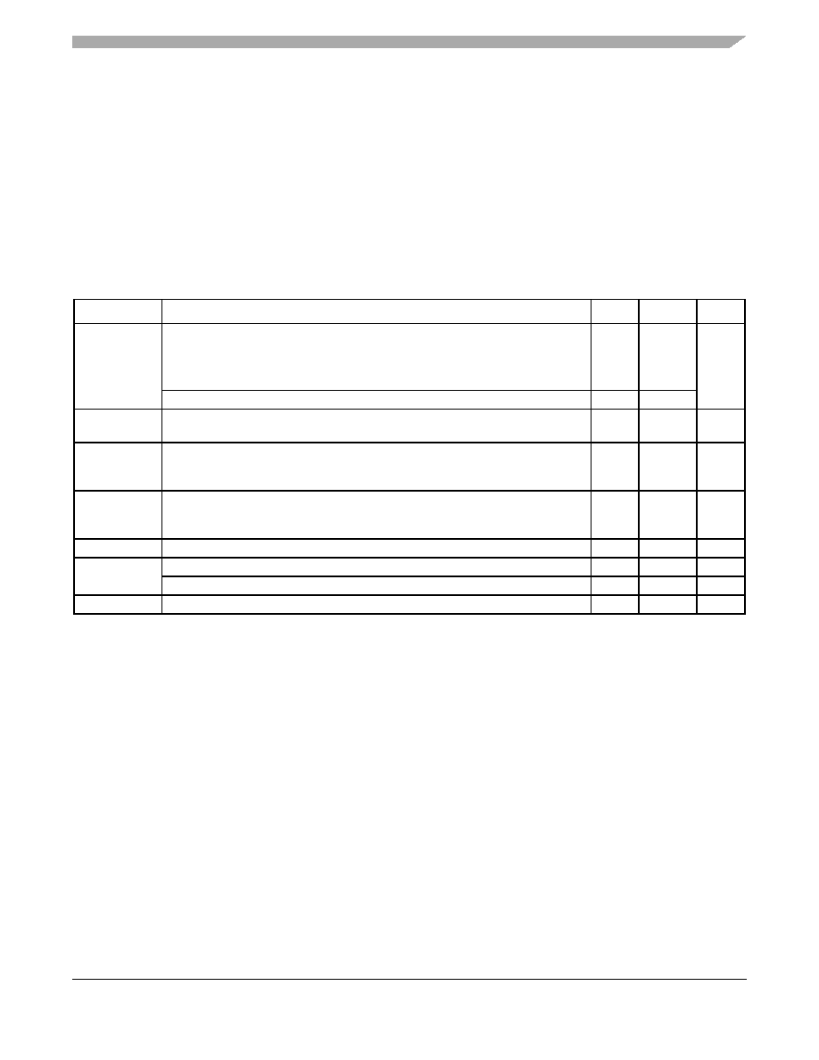
Table 8 provides the operating ranges.
NOTE
The term NVCC in this section refers to the associated supply rail of an
input or output. The association is shown in the Signal Multiplexing chapter
of the reference manual.
CAUTION
NVCC6 and NVCC9 must be at the same voltage potential. These supplies
are connected together on-chip to optimize ESD damage immunity.
Table 8. Operating Ranges
Symbol
Parameter
Min
Max
Units
QVCC,
QVCC1,
QVCC4
Core Operating Voltage1,2,3
1 Measured at package balls, including peripherals, ARM, and L2 cache supplies (QVCC, QVCC1, QVCC4, respectively).
2
The core voltage must be higher than 1.38V to avoid corrupted data during transfers from the USB HS. Please refer to Errata
file ENGcm02610 ID.
3
If the Core voltage is supplied by the MC13738, it will be 1.6 ± 0.05 V during the power-up sequence. This is allowed. After
power-up the voltage should be reduced to avoid operation in overdrive mode.
V
Silicon rev 1.15, 1.2, and 2.0
0
≤ f
ARM ≤ 400 MHz, non-overdrive
0
≤ f
ARM ≤ 400 MHz, overdrive
4
0
≤ f
ARM ≤ 532 MHz, overdrive
4 Supply voltage is considered “overdrive” for voltages above 1.47 V. Operation time in overdrive—whether switching or
not—must be limited to a cumulative duration of 1.25 years (10,950 hours) or less to sustain the maximum operating voltage
without significant device degradation—for example, 25% (average 6 hours out of 24 yours per day) duty cycle for 5-year rated
equipment. To tolerate the maximum operating overdrive voltage for 10 years, the device must have a duty cycle of 12.5% or
less in overdrive (for example 3 out of 24 hours per day). Below 1.47V, duty cycle restrictions may apply for equipment rated
above 5 years.
1.22
>1.47
1.55
1.47
1.65
State Retention Voltage5
5 The SR voltage is applied to QVCC, QVCC1, and QVCC4 after the device is placed in SR mode. The Real-Time Clock (RTC)
is operational in State Retention (SR) mode.
0.95
—
NVCC1,
NVCC3–10
I/O Supply Voltage, except DDR6non-overdrive
overdrive7
6 Overshoot and undershoot conditions (transitions above NVCC and below GND) on I/O must be held below 0.6 V, and the
duration of the overshoot/undershoot must not exceed 10% of the system clock cycle. Overshoot/undershoot must be
controlled through printed circuit board layout, transmission line impedance matching, signal line termination, or other
methods. Non-compliance to this specification may affect device reliability or cause permanent damage to the device.
1.75
>3.1
3.1
3.3
V
NVCC2,
NVCC21,
NVCC22
I/O Supply Voltage, DDR only
1.75
1.95
V
FVCC, MVCC,
SVCC, UVCC
PLL (Phase-Locked Loop) and FPM (Frequency Pre-multiplier) Supply Voltage8
non-overdrive
overdrive4
1.3
>1.47
1.47
1.6
V
IOQVDD
On-device Level Shifter Supply Voltage
1.6
1.9
V
FUSE_VDD
Fusebox read Supply Voltage9, 10
1.65
1.95
V
Fusebox write (program) Supply Voltage11
3.0
3.3
V
TA
Operating Ambient Temperature Range12
070
oC
Because
of
an
order
from
the
United
States
International
Trade
Commission,
BGA-packaged
product
lines
and
part
numbers
indicated
here
currently
are
not
available
from
Freescale
for
import
or
sale
in
the
United
States
prior
to
September
2010:
i.MX31
Product
Family
相关PDF资料 |
PDF描述 |
|---|---|
| 501798-4 | BULKHEAD ASSY., FSD, TYPE S |
| 1588172-3 | MPO ADAPTER ASSY. W/O FLANGE |
| 1588172-1 | MPO ADAPTER ASSY.AND RETENTION |
| 1374352-1 | ADAPTER, DUPL, LC, BLUE |
| 1588172-6 | MPO ADAPTER W/FLANGE AND CLIP |
相关代理商/技术参数 |
参数描述 |
|---|---|
| MCIMX31LVKN5BR2 | 功能描述:IC MPU MAP I.MX31L 457-MAPBGA RoHS:是 类别:集成电路 (IC) >> 嵌入式 - 微控制器, 系列:i.MX31 标准包装:1 系列:AVR® ATmega 核心处理器:AVR 芯体尺寸:8-位 速度:16MHz 连通性:I²C,SPI,UART/USART 外围设备:欠压检测/复位,POR,PWM,WDT 输入/输出数:32 程序存储器容量:32KB(16K x 16) 程序存储器类型:闪存 EEPROM 大小:1K x 8 RAM 容量:2K x 8 电压 - 电源 (Vcc/Vdd):2.7 V ~ 5.5 V 数据转换器:A/D 8x10b 振荡器型:内部 工作温度:-40°C ~ 125°C 封装/外壳:44-TQFP 包装:剪切带 (CT) 其它名称:ATMEGA324P-B15AZCT |
| MCIMX31LVKN5C | 功能描述:IC MPU MAP I.MX31L 457-MAPBGA RoHS:是 类别:集成电路 (IC) >> 嵌入式 - 微控制器, 系列:i.MX31 标准包装:1 系列:AVR® ATmega 核心处理器:AVR 芯体尺寸:8-位 速度:16MHz 连通性:I²C,SPI,UART/USART 外围设备:欠压检测/复位,POR,PWM,WDT 输入/输出数:32 程序存储器容量:32KB(16K x 16) 程序存储器类型:闪存 EEPROM 大小:1K x 8 RAM 容量:2K x 8 电压 - 电源 (Vcc/Vdd):2.7 V ~ 5.5 V 数据转换器:A/D 8x10b 振荡器型:内部 工作温度:-40°C ~ 125°C 封装/外壳:44-TQFP 包装:剪切带 (CT) 其它名称:ATMEGA324P-B15AZCT |
| MCIMX31LVKN5CR2 | 功能描述:IC MPU MAP I.MX31L 457-MAPBGA RoHS:是 类别:集成电路 (IC) >> 嵌入式 - 微控制器, 系列:i.MX31 标准包装:1 系列:AVR® ATmega 核心处理器:AVR 芯体尺寸:8-位 速度:16MHz 连通性:I²C,SPI,UART/USART 外围设备:欠压检测/复位,POR,PWM,WDT 输入/输出数:32 程序存储器容量:32KB(16K x 16) 程序存储器类型:闪存 EEPROM 大小:1K x 8 RAM 容量:2K x 8 电压 - 电源 (Vcc/Vdd):2.7 V ~ 5.5 V 数据转换器:A/D 8x10b 振荡器型:内部 工作温度:-40°C ~ 125°C 封装/外壳:44-TQFP 包装:剪切带 (CT) 其它名称:ATMEGA324P-B15AZCT |
| MCIMX31LVKN5R2 | 功能描述:IC MPU MAP I.MX31L 457-MAPBGA RoHS:是 类别:集成电路 (IC) >> 嵌入式 - 微控制器, 系列:i.MX31 标准包装:1 系列:87C 核心处理器:MCS 51 芯体尺寸:8-位 速度:16MHz 连通性:SIO 外围设备:- 输入/输出数:32 程序存储器容量:8KB(8K x 8) 程序存储器类型:OTP EEPROM 大小:- RAM 容量:256 x 8 电压 - 电源 (Vcc/Vdd):4 V ~ 6 V 数据转换器:- 振荡器型:外部 工作温度:0°C ~ 70°C 封装/外壳:44-DIP 包装:管件 其它名称:864285 |
| MCIMX31LVMN5C | 功能描述:IC MPU MAP I.MX31L 473-MAPBGA RoHS:是 类别:集成电路 (IC) >> 嵌入式 - 微控制器, 系列:i.MX31 标准包装:1 系列:AVR® ATmega 核心处理器:AVR 芯体尺寸:8-位 速度:16MHz 连通性:I²C,SPI,UART/USART 外围设备:欠压检测/复位,POR,PWM,WDT 输入/输出数:32 程序存储器容量:32KB(16K x 16) 程序存储器类型:闪存 EEPROM 大小:1K x 8 RAM 容量:2K x 8 电压 - 电源 (Vcc/Vdd):2.7 V ~ 5.5 V 数据转换器:A/D 8x10b 振荡器型:内部 工作温度:-40°C ~ 125°C 封装/外壳:44-TQFP 包装:剪切带 (CT) 其它名称:ATMEGA324P-B15AZCT |
发布紧急采购,3分钟左右您将得到回复。