- 您现在的位置:买卖IC网 > PDF目录10950 > MCIMX355AVM4BR2 (Freescale Semiconductor)IC MPU I.MX35 400MAPBGA PDF资料下载
参数资料
| 型号: | MCIMX355AVM4BR2 |
| 厂商: | Freescale Semiconductor |
| 文件页数: | 24/147页 |
| 文件大小: | 0K |
| 描述: | IC MPU I.MX35 400MAPBGA |
| 标准包装: | 1,000 |
| 系列: | i.MX35 |
| 核心处理器: | ARM11 |
| 芯体尺寸: | 32-位 |
| 速度: | 400MHz |
| 连通性: | 1 线,CAN,EBI/EMI,以太网,I²C,MMC,SPI,SSI,UART/USART,USB OTG |
| 外围设备: | DMA,I²S,LCD,POR,PWM,WDT |
| 输入/输出数: | 96 |
| 程序存储器类型: | ROMless |
| RAM 容量: | 128K x 8 |
| 电压 - 电源 (Vcc/Vdd): | 1.22 V ~ 1.47 V |
| 振荡器型: | 外部 |
| 工作温度: | -40°C ~ 85°C |
| 封装/外壳: | 400-LFBGA |
| 包装: | 带卷 (TR) |
第1页第2页第3页第4页第5页第6页第7页第8页第9页第10页第11页第12页第13页第14页第15页第16页第17页第18页第19页第20页第21页第22页第23页当前第24页第25页第26页第27页第28页第29页第30页第31页第32页第33页第34页第35页第36页第37页第38页第39页第40页第41页第42页第43页第44页第45页第46页第47页第48页第49页第50页第51页第52页第53页第54页第55页第56页第57页第58页第59页第60页第61页第62页第63页第64页第65页第66页第67页第68页第69页第70页第71页第72页第73页第74页第75页第76页第77页第78页第79页第80页第81页第82页第83页第84页第85页第86页第87页第88页第89页第90页第91页第92页第93页第94页第95页第96页第97页第98页第99页第100页第101页第102页第103页第104页第105页第106页第107页第108页第109页第110页第111页第112页第113页第114页第115页第116页第117页第118页第119页第120页第121页第122页第123页第124页第125页第126页第127页第128页第129页第130页第131页第132页第133页第134页第135页第136页第137页第138页第139页第140页第141页第142页第143页第144页第145页第146页第147页
i.MX35 Applications Processors for Automotive Products, Rev. 10
Freescale Semiconductor
12
3
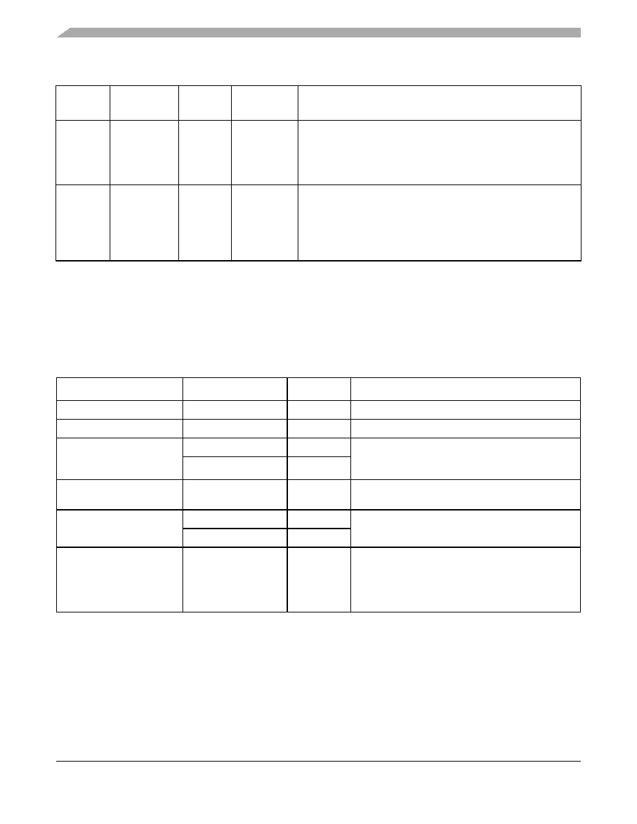
Signal Descriptions: Special Function Related Pins
Some special functional requirements are supported in the device. The details about these special functions
and the corresponding pin names are listed in Table 5.
USBOH
High-speed
USB on-the-go
SDMA
Connectivity
peripherals
The USB module provides high performance USB on-the-go (OTG)
functionality (up to 480 Mbps), compliant with the USB 2.0
specification, the OTG supplement, and the ULPI 1.0 low pin count
specification. The module has DMA capabilities handling data
transfer between internal buffers and system memory.
WDOG
Watchdog
modules
ARM
Timer
peripherals
Each module protects against system failures by providing a method
of escaping from unexpected events or programming errors. Once
activated, the timer must be serviced by software on a periodic
basis. If servicing does not take place, the watchdog times out and
then either asserts a system reset signal or an interrupt request
signal, depending on the software configuration.
1 ARM = ARM1136 platform, SDMA = SDMA platform
Table 5. Special Function Related Pins
Function Name
Pin Name
Mux Mode
Detailed Description
External ARM Clock
EXT_ARMCLK
ALT0
External clock input for ARM clock.
External Peripheral Clock
I2C1_CLK
ALT6
External peripheral clock source.
External 32-kHz Clock
CAPTURE
ALT4
External clock input of 32 kHz, used when the internal
24M Oscillator is powered off, which could be
configured either from CAPTURE or CSPI1_SS1.
CSPI1_SS1
ALT2
Clock Out
CLKO
ALT0
Clock-out pin from CCM, clock source is controllable
and can also be used for debug.
Power Ready
GPIO1_0
ALT1
PMIC power-ready signal, which can be configured
either from GPIO1_0 or TX1.
TX1
ALT1
Tamper Detect
GPIO1_1
ALT6
Tamper-detect logic is used to issue a security
violation. This logic is activated if the tamper-detect
input is asserted. Tamper-detect logic is enabled by the
bit of IOMUXC_GPRA[2]. After enabling the logic, it is
impossible to disable it until the next reset.
Table 4. Digital and Analog Modules (continued)
Block
Mnemonic
Block Name
Domain1
Subsystem
Brief Description
相关PDF资料 |
PDF描述 |
|---|---|
| MCIMX355AJQ5CR2 | MULTIMEDIA PROCESSOR 400-MAPBGA |
| IDT821054PQFG | IC PCM CODEC QUAD MPI 64-PQFP |
| MCIMX357CVM5BR2 | IC MPU I.MX35 400MAPBGA |
| MCIMX357CVM5B | IC MPU I.MX35 400MAPBGA |
| MCIMX357CJQ5CR2 | MULTIMEDIA PROCESSOR 400-MAPBGA |
相关代理商/技术参数 |
参数描述 |
|---|---|
| MCIMX355AVM5B | 功能描述:处理器 - 专门应用 RINGO MX35 TO2 RoHS:否 制造商:Freescale Semiconductor 类型:Multimedia Applications 核心:ARM Cortex A9 处理器系列:i.MX6 数据总线宽度:32 bit 最大时钟频率:1 GHz 指令/数据缓存: 数据 RAM 大小:128 KB 数据 ROM 大小: 工作电源电压: 最大工作温度:+ 95 C 安装风格:SMD/SMT 封装 / 箱体:MAPBGA-432 |
| MCIMX355AVM5BR2 | 功能描述:处理器 - 专门应用 RINGO MX35 TO2 RoHS:否 制造商:Freescale Semiconductor 类型:Multimedia Applications 核心:ARM Cortex A9 处理器系列:i.MX6 数据总线宽度:32 bit 最大时钟频率:1 GHz 指令/数据缓存: 数据 RAM 大小:128 KB 数据 ROM 大小: 工作电源电压: 最大工作温度:+ 95 C 安装风格:SMD/SMT 封装 / 箱体:MAPBGA-432 |
| MCIMX356AJM5B | 功能描述:开发板和工具包 - ARM RINGO MX35 TO2 RoHS:否 制造商:Arduino 产品:Development Boards 工具用于评估:ATSAM3X8EA-AU 核心:ARM Cortex M3 接口类型:DAC, ICSP, JTAG, UART, USB 工作电源电压:3.3 V |
| MCIMX356AJM5BR2 | 功能描述:处理器 - 专门应用 RINGO MX35 TO2 RoHS:否 制造商:Freescale Semiconductor 类型:Multimedia Applications 核心:ARM Cortex A9 处理器系列:i.MX6 数据总线宽度:32 bit 最大时钟频率:1 GHz 指令/数据缓存: 数据 RAM 大小:128 KB 数据 ROM 大小: 工作电源电压: 最大工作温度:+ 95 C 安装风格:SMD/SMT 封装 / 箱体:MAPBGA-432 |
| MCIMX356AJQ4C | 制造商:FREESCALE 制造商全称:Freescale Semiconductor, Inc 功能描述:i.MX35 Applications Processors for Automotive Products |
发布紧急采购,3分钟左右您将得到回复。