- 您现在的位置:买卖IC网 > PDF目录16523 > MCP1316T-29LE/OT (Microchip Technology)IC SUPERVISOR 2.90V P-P SOT23-5 PDF资料下载
参数资料
| 型号: | MCP1316T-29LE/OT |
| 厂商: | Microchip Technology |
| 文件页数: | 31/52页 |
| 文件大小: | 0K |
| 描述: | IC SUPERVISOR 2.90V P-P SOT23-5 |
| 标准包装: | 1 |
| 类型: | 简单复位/加电复位 |
| 监视电压数目: | 1 |
| 输出: | 推挽式,图腾柱 |
| 复位: | 低有效 |
| 复位超时: | 最小为 140 ms |
| 电压 - 阀值: | 2.9V |
| 工作温度: | -40°C ~ 125°C |
| 安装类型: | 表面贴装 |
| 封装/外壳: | SC-74A,SOT-753 |
| 供应商设备封装: | SOT-23-5 |
| 包装: | 标准包装 |
| 产品目录页面: | 662 (CN2011-ZH PDF) |
| 其它名称: | MCP1316T-29LE/OTDKR |
第1页第2页第3页第4页第5页第6页第7页第8页第9页第10页第11页第12页第13页第14页第15页第16页第17页第18页第19页第20页第21页第22页第23页第24页第25页第26页第27页第28页第29页第30页当前第31页第32页第33页第34页第35页第36页第37页第38页第39页第40页第41页第42页第43页第44页第45页第46页第47页第48页第49页第50页第51页第52页
�� �
�
�MCP131X/2X�
�4.1.1�
�POWER-UP/RISING� V� DD�
�4.1.2�
�POWER-DOWN/BROWN-OUTS�
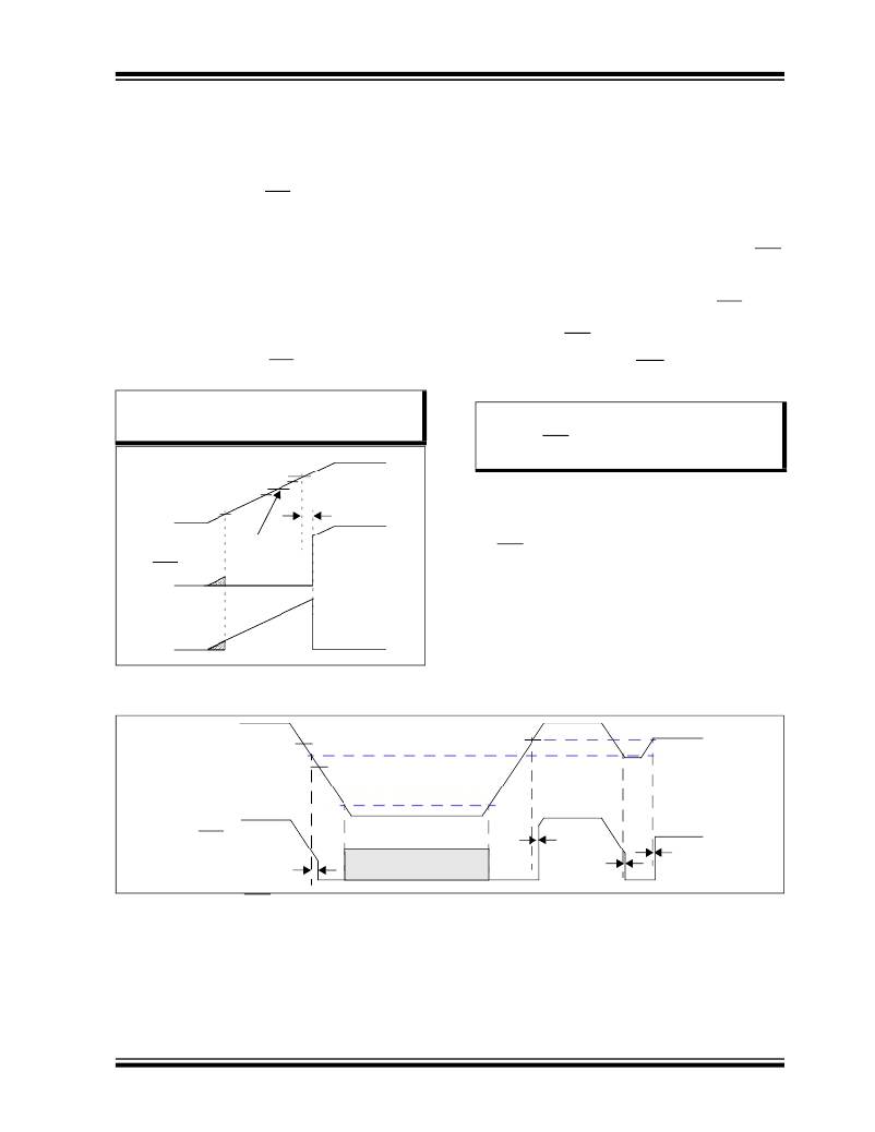
�As� the� device� V� DD� rises,� the� device’s� Reset� circuit� will�
�remain� active� until� the� voltage� rises� above� the� “actual”�
�trip� point� (V� TRIP� )� plus� the� hysteresis� (V� HYS� ).�
��waveform� of� the� RST� and� RST� pins.�
�As� the� device� powers� up,� the� voltage� will� start� below�
�the� valid� operating� voltage� of� the� device.� At� this�
�voltage,� the� Reset� output� value� is� not� valid.� Once� the�
�voltage� is� above� the� minimum� operating� voltage� (1V)�
�and� below� the� selected� V� TRIP� ,� the� Reset� output� will� be�
�active.�
�Once� the� device� voltage� rises� above� the� “actual”� trip�
�point� (V� TRIP� )� plus� the� hysteresis� (V� HYS� ),� the� Reset� delay�
�timer� (t� RST� )� starts.� When� the� Reset� delay� timer� times�
�As� the� device� powers-down/brown-outs,� the� voltage�
�(V� DD� )� falls� from� a� voltage� above� the� device’s� trip� point�
�(V� TRIP� ).� The� device’s� “actual”� trip� point� voltage� (V� TRIP� )�
�will� be� between� the� minimum� trip� point� (V� TRIPMIN� )� and�
�the� maximum� trip� point� (V� TRIPMAX� ).� Once� the� device�
�voltage� (V� DD� )� goes� below� this� voltage,� the� Reset� pin(s)�
�will� be� forced� to� the� active� state.� There� is� a� hysteresis�
�on� this� trip� point.� This� is� so� that� noise� on� the� device�
�voltage� (V� DD� )� does� not� cause� the� Reset� pin� (RST/RST)�
�to� “jitter”� (change� between� driving� an� active� and�
�inactive).�
��determined� by� t� he V� DD� voltage,� while� Table� 4-1� shows�
�the� state� of� the� RST� pin.�
�out,� the� Reset� output� (RST/RST)� is� driven� inactive.�
�4.1.2.1�
�Operation� of� RST� pin� with� Internal�
�Pull-Up� Resistor�
�Note:�
�While� the� Reset� delay� timer� (t� RST� )� is�
�active,� additional� system� current� is�
�consumed.�
�Note:�
�Only� the� MCP1316M,� MCP1318M� and�
�MCP1319M� devices� have� an� open-drain�
�RST� output� pin� with� an� internal� pull-up�
�resistor.�
�V� TRIPMAX�
�V� TRIPMIN�
�V� TRIP� +� V� HYS�
�The� internal� pull-up� resistor� has� a� typical� value� of�
�4.7� k� Ω� .� The� internal� pull-up� eliminates� the� need� for� an�
�V� DD�
�1V�
�V� TRIP�
�t� RST�
�external� resistor.�
�To� reduce� the� current� consumption� of� the� device,� when�
�the� RST� pin� is� driving� low,� the� resistor� is� disconnected.�
�RST�
�RST�
�FIGURE� 4-13:�
�Power-up.�
�Reset� Pin� Operation� on� a�
�V� DD�
�V� TRIPMAX�
�V� TRIPMIN�
�V� TRIP� +� V� HYS�
�V� TRIP�
�V� TRIP�
�1V�
�RST�
�t� RPD�
�<� 1V� is� outside� the�
�device� specifications�
�t� RST�
�t� RPD�
�t� RST�
�FIGURE� 4-14:�
�RST� Operation� as� Determined� by� the� V� TRIP� and� V� HYS� .�
�?� 2005-2012� Microchip� Technology� Inc.�
�DS21985C-page� 31�
�相关PDF资料 |
PDF描述 |
|---|---|
| VE-JVP-EZ-S | CONVERTER MOD DC/DC 13.8V 25W |
| UPM1K560MPD1TD | CAP ALUM 56UF 80V 20% RADIAL |
| GMM11DRTN-S13 | CONN EDGECARD 22POS .156 EXTEND |
| AQ1057N5J-T | INDUCTOR 7.5NH 400MA 0402 SMD |
| XR16V2651IM-0B-EB | EVAL BOARD FOR V2651 48TQFP |
相关代理商/技术参数 |
参数描述 |
|---|---|
| MCP1316T-29NE/OT | 功能描述:监控电路 ACTIVE LOW P-P WDI RoHS:否 制造商:STMicroelectronics 监测电压数: 监测电压: 欠电压阈值: 过电压阈值: 输出类型:Active Low, Open Drain 人工复位:Resettable 监视器:No Watchdog 电池备用开关:No Backup 上电复位延迟(典型值):10 s 电源电压-最大:5.5 V 最大工作温度:+ 85 C 安装风格:SMD/SMT 封装 / 箱体:UDFN-6 封装:Reel |
| MCP1316T-46BE/OT | 功能描述:监控电路 ACTIVE LOW P-P WDI RoHS:否 制造商:STMicroelectronics 监测电压数: 监测电压: 欠电压阈值: 过电压阈值: 输出类型:Active Low, Open Drain 人工复位:Resettable 监视器:No Watchdog 电池备用开关:No Backup 上电复位延迟(典型值):10 s 电源电压-最大:5.5 V 最大工作温度:+ 85 C 安装风格:SMD/SMT 封装 / 箱体:UDFN-6 封装:Reel |
| MCP1316T-46FE/OT | 功能描述:监控电路 ACTIVE LOW P-P WDI RoHS:否 制造商:STMicroelectronics 监测电压数: 监测电压: 欠电压阈值: 过电压阈值: 输出类型:Active Low, Open Drain 人工复位:Resettable 监视器:No Watchdog 电池备用开关:No Backup 上电复位延迟(典型值):10 s 电源电压-最大:5.5 V 最大工作温度:+ 85 C 安装风格:SMD/SMT 封装 / 箱体:UDFN-6 封装:Reel |
| MCP1316T-46KE/OT | 制造商:Microchip Technology Inc 功能描述: |
| MCP1316T-46LE/OT | 功能描述:监控电路 Active low P-P RoHS:否 制造商:STMicroelectronics 监测电压数: 监测电压: 欠电压阈值: 过电压阈值: 输出类型:Active Low, Open Drain 人工复位:Resettable 监视器:No Watchdog 电池备用开关:No Backup 上电复位延迟(典型值):10 s 电源电压-最大:5.5 V 最大工作温度:+ 85 C 安装风格:SMD/SMT 封装 / 箱体:UDFN-6 封装:Reel |
发布紧急采购,3分钟左右您将得到回复。