- 您现在的位置:买卖IC网 > PDF目录14482 > MCP1602-120I/MF (Microchip Technology)IC REG BUCK SYNC 1.2V 0.5A 8DFN PDF资料下载
参数资料
| 型号: | MCP1602-120I/MF |
| 厂商: | Microchip Technology |
| 文件页数: | 12/26页 |
| 文件大小: | 0K |
| 描述: | IC REG BUCK SYNC 1.2V 0.5A 8DFN |
| 标准包装: | 120 |
| 类型: | 降压(降压) |
| 输出类型: | 固定 |
| 输出数: | 1 |
| 输出电压: | 1.2V |
| 输入电压: | 2.7 V ~ 5.5 V |
| 频率 - 开关: | 2MHz |
| 电流 - 输出: | 500mA |
| 同步整流器: | 是 |
| 工作温度: | -40°C ~ 85°C |
| 安装类型: | 表面贴装 |
| 封装/外壳: | 8-VDFN 裸露焊盘 |
| 包装: | 管件 |
| 供应商设备封装: | 8-DFN-EP(3x3) |
| 产品目录页面: | 668 (CN2011-ZH PDF) |
�� �
�
�MCP1602�
�4.0�
�DETAILED� DESCRIPTION�
�4.1�
�Device� Overview�
�PFM-to-PWM� mode� transition� is� initiated� for� any� of� the�
�The� MCP1602� is� a� synchronous� buck� regulator� with� a�
�power-good� signal.� The� device� operates� in� a� Pulse�
�Frequency� Modulation� (PFM)� mode� or� a� Pulse� Width�
�following� conditions:�
�?� Continuous� device� switching�
�?� Output� voltage� has� dropped� out� of� regulation�
�Modulation� (PWM)� mode� to� maximize� system�
�efficiency� over� the� entire� operating� current� range.�
�4.2.2�
�LIGHT� LOAD,� PFM� MODE�
�Capable� of� operating� from� a� 2.7V� to� 5.5V� input� voltage�
�source,� the� MCP1602� can� deliver� 500� mA� of�
�continuous� output� current.�
�When� using� the� MCP1602,� the� PCB� area� required� for�
�a� complete� step-down� converter� is� minimized� since�
�both� the� main� P-Channel� MOSFET� and� the� synchro-�
�nous� N-Channel� MOSFET� are� integrated.� Also� while� in�
�PWM� mode,� the� device� switches� at� a� constant�
�frequency� of� 2.0� MHz� (typical)� which� allow� for� small� fil-�
�tering� components.� Both� fixed� and� adjustable� output�
�voltage� options� are� available.� The� fixed� voltage� options�
�(1.2V,� 1.5V,� 1.8V,� 2.5V,� 3.3V)� do� not� require� an� external�
�voltage� divider� which� further� reduces� the� required�
�During� light� load� conditions,� the� MCP1602� operates� in�
�a� PFM� mode.� When� the� MCP1602� enters� this� mode,� it�
�begins� to� skip� pulses� to� minimize� unnecessary�
�quiescent� current� draw� by� reducing� the� number� of�
�switching� cycles� per� second.� The� typical� quiescent�
�current� draw� for� this� device� is� 45� μA.�
�PWM-to-PFM� mode� transition� is� initiated� for� any� of� the�
�following� conditions:�
�?� Discontinuous� inductor� current� is� sensed� for� a� set�
�duration�
�?� Inductor� peak� current� falls� below� the� transition�
�threshold� limit�
�circuit� board� footprint.� The� adjustable� output� voltage�
�options� allow� for� more� flexibility� in� the� design,� but�
�4.3�
�Power-Good� (PG)�
�require� an� external� voltage� divider.�
�Additionally� the� device� features� undervoltage� lockout�
�(UVLO),� overtemperature� shutdown,� overcurrent�
�protection,� and� enable/disable� control.�
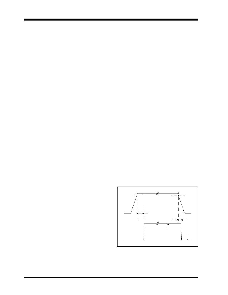
�The� open-drain� power-good� (PG)� circuitry� monitors� the�
�regulated� output� voltage.� A� fixed� delay� time� of�
�approximately� 262� ms� is� generated� once� the� output�
�voltage� is� above� the� power-good� high� threshold,�
�4.2�
�Synchronous� Buck� Regulator�
�V� TH_H� ,� (typically� 94%� of� V� OUT� ).� As� the� output� voltage�
�falls� below� the� power-good� low� threshold,� V� TH_L� ,�
�The� MCP1602� has� two� distinct� modes� of� operation� that�
�allow� the� device� to� maintain� a� high� level� of� efficiency�
�throughout� the� entire� operating� current� and� voltage�
�range.� The� device� automatically� switches� between�
�PWM� mode� and� PFM� mode� depending� upon� the� output�
�load� requirements.�
�(typically� 92%� of� V� OUT� )� the� PG� signal� transitions� to� a�
�low� state� indicating� that� the� output� is� out� of� regulation.�
�The� PG� circuitry� has� a� typical� 165� μs� delay� when�
�detecting� a� falling� output� voltage.� This� helps� to�
�increase� the� noise� immunity� of� the� power-good� output,�
�avoiding� false� triggering� of� the� PG� signal� during� line�
�and� load� transients.�
�4.2.1�
�FIXED� FREQUENCY,� PWM� MODE�
�During� heavy� load� conditions,� the� MCP1602� operates�
�V� TH_H�
�at� a� high,� fixed� switching� frequency� of� 2.0� MHz� (typi-�
�cal).� This� minimizes� output� ripple� (10� -� 15� mV� typically)�
�and� noise� while� maintaining� high� efficiency� (88%� typi-�
�cal� with� V� IN� =� 3.6V,� V� OUT� =� 1.8V,� I� OUT� =� 300� mA).�
�During� normal� PWM� operation,� the� beginning� of� a�
�switching� cycle� occurs� when� the� internal� P-Channel�
�MOSFET� is� turned� on.� The� ramping� inductor� current� is�
�sensed� and� tied� to� one� input� of� the� internal� high-speed�
�V� OUT�
�t� RPU�
�V� TH_L�
�t� RPD�
�comparator.� The� other� input� to� the� high-speed� compar-�
�ator� is� the� error� amplifier� output.� This� is� the� difference�
�PG�
�V� OH�
�V� OL�
�between� the� internal� 0.8V� reference� and� the� sensed�
�output� voltage.� When� the� sensed� current� becomes�
�equal� to� the� amplified� error� signal,� the� high-speed�
�comparator� switches� states� and� the� P-Channel�
�MOSFET� is� turned� off.� The� N-Channel� MOSFET� is�
�turned� on� until� the� internal� oscillator� sets� an� internal� RS�
�latch� initiating� the� beginning� of� another� switching� cycle.�
�DS22061A-page� 12�
�FIGURE� 4-1:�
�Power-Good� Timing.�
�?� 2007� Microchip� Technology� Inc.�
�相关PDF资料 |
PDF描述 |
|---|---|
| VE-BW1-EX-F1 | CONVERTER MOD DC/DC 12V 75W |
| TPS62231DRYT | IC REG BUCK SYNC 1.8V 0.5A 6SON |
| 2300HT-2R7-H-RC | INDUCTOR TOROID 2.7UH 15% HORZ |
| VE-BW1-EW-F3 | CONVERTER MOD DC/DC 12V 100W |
| EYM28DTBN-S189 | CONN EDGECARD 56POS R/A .156 SLD |
相关代理商/技术参数 |
参数描述 |
|---|---|
| MCP1602-150I/MF | 功能描述:开关变换器、稳压器与控制器 20MHz 05A Synch-Buck PFM/PWM Reg RoHS:否 制造商:Texas Instruments 输出电压:1.2 V to 10 V 输出电流:300 mA 输出功率: 输入电压:3 V to 17 V 开关频率:1 MHz 工作温度范围: 安装风格:SMD/SMT 封装 / 箱体:WSON-8 封装:Reel |
| MCP1602-150I/MS | 功能描述:开关变换器、稳压器与控制器 20MHz 05A Synch-Buck PFM/PWM Reg RoHS:否 制造商:Texas Instruments 输出电压:1.2 V to 10 V 输出电流:300 mA 输出功率: 输入电压:3 V to 17 V 开关频率:1 MHz 工作温度范围: 安装风格:SMD/SMT 封装 / 箱体:WSON-8 封装:Reel |
| MCP1602-180I/MF | 功能描述:开关变换器、稳压器与控制器 20MHz 05A Synch-Buck PFM/PWM Reg RoHS:否 制造商:Texas Instruments 输出电压:1.2 V to 10 V 输出电流:300 mA 输出功率: 输入电压:3 V to 17 V 开关频率:1 MHz 工作温度范围: 安装风格:SMD/SMT 封装 / 箱体:WSON-8 封装:Reel |
| MCP1602-180I/MS | 功能描述:开关变换器、稳压器与控制器 20MHz 05A Synch-Buck PFM/PWM Reg RoHS:否 制造商:Texas Instruments 输出电压:1.2 V to 10 V 输出电流:300 mA 输出功率: 输入电压:3 V to 17 V 开关频率:1 MHz 工作温度范围: 安装风格:SMD/SMT 封装 / 箱体:WSON-8 封装:Reel |
| MCP1602-250I/MF | 功能描述:开关变换器、稳压器与控制器 20MHz 05A Synch-Buck PFM/PWM Reg RoHS:否 制造商:Texas Instruments 输出电压:1.2 V to 10 V 输出电流:300 mA 输出功率: 输入电压:3 V to 17 V 开关频率:1 MHz 工作温度范围: 安装风格:SMD/SMT 封装 / 箱体:WSON-8 封装:Reel |
发布紧急采购,3分钟左右您将得到回复。