- 您现在的位置:买卖IC网 > PDF目录1852 > MCP16323T-500E/NG (Microchip Technology)IC REG BUCK SYNC 5V 3A 16-VQFN PDF资料下载
参数资料
| 型号: | MCP16323T-500E/NG |
| 厂商: | Microchip Technology |
| 文件页数: | 21/32页 |
| 文件大小: | 0K |
| 描述: | IC REG BUCK SYNC 5V 3A 16-VQFN |
| 标准包装: | 1 |
| 类型: | 降压(降压) |
| 输出类型: | 固定 |
| 输出数: | 1 |
| 输出电压: | 5V |
| 输入电压: | 6 V ~ 18 V |
| PWM 型: | 电流模式 |
| 频率 - 开关: | 1MHz |
| 电流 - 输出: | 3A |
| 同步整流器: | 是 |
| 工作温度: | -40°C ~ 125°C |
| 安装类型: | 表面贴装 |
| 封装/外壳: | 16-VFQFN 裸露焊盘 |
| 包装: | 标准包装 |
| 供应商设备封装: | 16-QFN(3x3) |
| 其它名称: | MCP16323T-500E/NGDKR |
第1页第2页第3页第4页第5页第6页第7页第8页第9页第10页第11页第12页第13页第14页第15页第16页第17页第18页第19页第20页当前第21页第22页第23页第24页第25页第26页第27页第28页第29页第30页第31页第32页
�� �
�
�MCP16323�
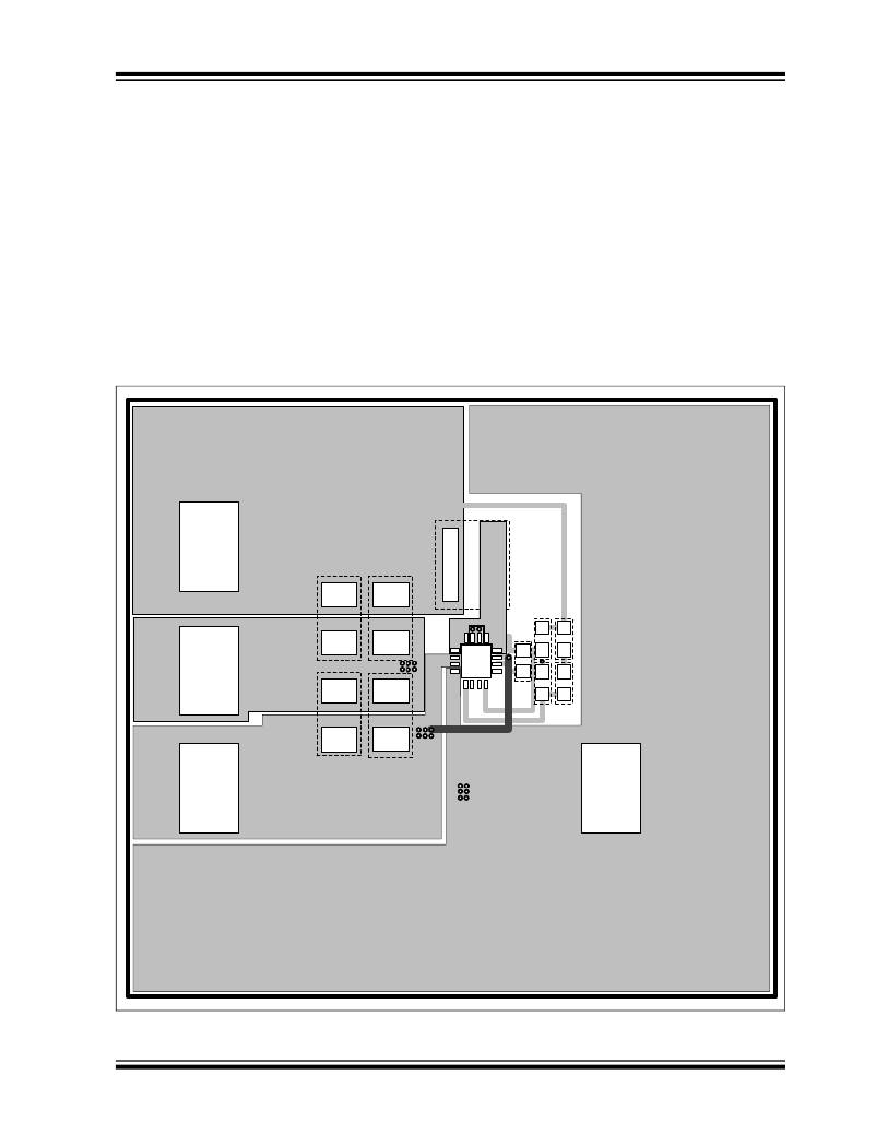
�5.0.9� PCB� LAYOUT� INFORMATION�
�Good� printed� circuit� board� layout� techniques� are�
�important� to� any� switching� circuitry,� and� switching�
�power� supplies� are� no� different.� When� wiring� the�
�switching� high-current� paths,� short� and� wide� traces�
�should� be� used.� Therefore,� it� is� important� that� the� input�
�and� output� capacitors� be� placed� as� close� as� possible� to�
�the� MCP16323� to� minimize� the� loop� area.�
�The� feedback� resistors� and� feedback� signal� should� be�
�routed� away� from� the� switching� node� and� the� switching�
�current� loop.� When� possible,� ground� planes� and� traces�
�should� be� used� to� help� shield� the� feedback� signal� and�
�minimize� noise� and� magnetic� interference.�
�A� good� MCP16323� layout� starts� with� C� IN� placement.�
�C� IN� supplies� current� to� the� input� of� the� circuit� when� the�
�switch� is� turned� on.� In� addition� to� supplying� high-�
�frequency� switch� current,� C� IN� also� provides� a� stable�
�voltage� source� for� the� internal� MCP16323� circuitry.�
�Unstable� PWM� operation� can� result� if� there� are�
�excessive� transients� or� ringing� on� the� V� IN� pin� of� the�
�MCP16323� device.� In� Figure� 5-1� ,� C� IN� is� placed� close� to�
�the� V� IN� pins.� A� ground� plane� on� the� bottom� of� the� board�
�provides� a� low� resistive� and� low� inductive� path� for� the�
�return� current.� The� next� priority� in� placement� is� the�
�freewheeling� current� loop� formed� by� C� OUT� and� L� while�
�strategically� placing� the� C� OUT� return� close� to� C� IN�
�return.� Next,� C� BOOST� should� be� placed� between� the�
�boost� pin� and� the� switch� node� pin.� This� leaves� space�
�close� to� the� MCP16323� V� FB� pin� to� place� R� TOP� and�
�R� BOT� .� R� TOP� and� R� BOT� are� routed� away� from� the� switch�
�node� so� noise� is� not� coupled� into� the� high-impedance�
�V� FB� input.�
�Top� layer� is� made�
�with� 2� oz� copper�
�The� 2� middle�
�layers� are� made�
�V� OUT�
�C� OUT�
�C� OUT�
�L�
�with� 1� oz� copper�
�and� connected� to�
�V� IN� and� GND�
�GND�
�R� PG�
�C� BOOST�
�10� Ω�
�MCP16323�
�Trace� on�
�R� BOT�
�R� TOP�
�V� IN�
�C� IN�
�C� IN�
�bottom� layer�
�GND�
�Bottom� layer� is� a� 2� oz�
�copper� ground� plane�
�Board� Dimensions�
�are� 2.5"� by� 2.5"�
�FIGURE� 5-1:�
�Recommended� Layout.�
�?� 2011� Microchip� Technology� Inc.�
�DS22284A-page� 21�
�相关PDF资料 |
PDF描述 |
|---|---|
| MCP1640C-I/MC | IC REG BOOST SYNC ADJ 0.1A 8DFN |
| MCP1653ST-E/UN | IC REG CTRLR BST FLYBK CM 10MSOP |
| MCP1700-3002E/TO | IC REG LDO 3V .25A TO-92-3 |
| MCP1701AT-4602I/MB | IC REG LDO 4.6V SOT89-3 |
| MCP1702T-1502E/MB | IC REG LDO 1.5V 50MA SOT89-3 |
相关代理商/技术参数 |
参数描述 |
|---|---|
| MCP16323T-ADJE/NG | 功能描述:开关变换器、稳压器与控制器 3A Synchrouns Buck Switcher 18Vin RoHS:否 制造商:Texas Instruments 输出电压:1.2 V to 10 V 输出电流:300 mA 输出功率: 输入电压:3 V to 17 V 开关频率:1 MHz 工作温度范围: 安装风格:SMD/SMT 封装 / 箱体:WSON-8 封装:Reel |
| MCP1632-BAE/MC | 制造商:Microchip Technology Inc 功能描述:STANDALONE LOW-SIDE PWM CONTROLLER WITH INTEGRATED MOSFET DR - Rail/Tube |
| MCP1632-BAE/MS | 制造商:Microchip Technology Inc 功能描述:STANDALONE LOW-SIDE PWM CONTROLLER WITH INTEGRATED MOSFET DR - Rail/Tube |
| MCP1640 | 制造商:MICROCHIP 制造商全称:Microchip Technology 功能描述:0.65V Start-up Synchronous Boost Regulator with True Output Disconnect or Input/Output Bypass Option |
| MCP1640_11 | 制造商:MICROCHIP 制造商全称:Microchip Technology 功能描述:0.65V Start-up Synchronous Boost Regulator with True Output Disconnect or Input/Output Bypass Option |
发布紧急采购,3分钟左右您将得到回复。