- 您现在的位置:买卖IC网 > PDF目录4994 > MCP1754ST-1802E/CB (Microchip Technology)IC REG LDO 1.8V .15A SOT-23A-3 PDF资料下载
参数资料
| 型号: | MCP1754ST-1802E/CB |
| 厂商: | Microchip Technology |
| 文件页数: | 5/42页 |
| 文件大小: | 0K |
| 描述: | IC REG LDO 1.8V .15A SOT-23A-3 |
| 标准包装: | 1 |
| 稳压器拓扑结构: | 正,固定式 |
| 输出电压: | 1.8V |
| 输入电压: | 3.6 V ~ 16 V |
| 电压 - 压降(标准): | 0.3V @ 150mA |
| 稳压器数量: | 1 |
| 电流 - 输出: | 150mA(最小) |
| 工作温度: | -40°C ~ 125°C |
| 安装类型: | 表面贴装 |
| 封装/外壳: | TO-236-3,SC-59,SOT-23-3 |
| 供应商设备封装: | SOT-23A-3 |
| 包装: | 标准包装 |
| 其它名称: | MCP1754ST-1802E/CBDKR |
第1页第2页第3页第4页当前第5页第6页第7页第8页第9页第10页第11页第12页第13页第14页第15页第16页第17页第18页第19页第20页第21页第22页第23页第24页第25页第26页第27页第28页第29页第30页第31页第32页第33页第34页第35页第36页第37页第38页第39页第40页第41页第42页
�� �
�
�MCP1754/MCP1754S�
�1.0�
�ELECTRICAL�
�CHARACTERISTICS�
�?� Notice:� Stresses� above� those� listed� under� “Maximum�
�Ratings”� may� cause� permanent� damage� to� the� device.� This� is�
�a� stress� rating� only� and� functional� operation� of� the� device� at�
�those� or� any� other� conditions� above� those� indicated� in� the�
�Absolute� Maximum� Ratings� ?�
�Input� Voltage,� V� IN� ..................................................................+� 17.6V�
�operational� listings� of� this� specification� is� not� implied.�
�Exposure� to� maximum� rating� conditions� for� extended� periods�
�may� affect� device� reliability.�
�VIN,� PWRGD,� SHDN� .....................� (GND-0.3V)� to� (V� IN� +0.3V)�
�VOUT� ..................................................� (GND-0.3V)� to� (+5.5V)�
��Output� Short� Circuit� Current� .................................� Continuous�
�Storage� temperature� .....................................-55°C� to� +150°C�
��Operating� Junction� Temperature...................-40°C� to� +150°C�
�ESD� protection� on� all� pins� ..........� ≥� 4� kV� HBM� and� ≥� 200V� MM�
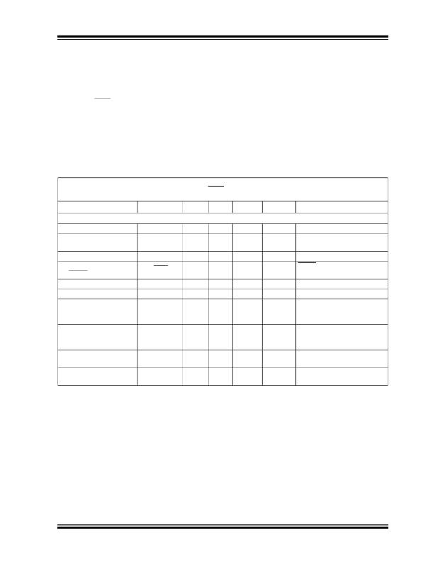
�AC/DC� CHARACTERISTICS�
�Electrical� Specifications:� Unless� otherwise� specified,� all� limits� are� established� for� V� IN� =� V� R� +� 1V,� Note� 1� ,� I� LOAD� =� 1� mA,� C� OUT� =�
�1� μF� (X7R),� C� IN� =� 1� μF� (X7R),� T� A� =� 25°C,� t� r(VIN)� =� 0.5V/μs,� SHDN� =� V� IN� ,� PWRGD� =� 10K� to� V� OUT� .�
�Boldface� type� applies� for� junction� temperatures,� T� J� (� Note� 7� )� of� -40°C� to� +125°C.�
�Parameters�
�Sym�
�Min�
�Typ�
�Max�
�Units�
�Conditions�
�Input� /� Output� Characteristics�
�Input� Operating� Voltage�
�Output� Voltage� Operating�
�V� IN�
�V� OUT-RANGE�
�3.6�
�1.8�
�—�
�—�
�16.0�
�5.5�
�V�
�V�
�Range�
�Input� Quiescent� Current�
�Input� Quiescent� Current�
�I� q�
�I� SHDN�
�—�
�—�
�56�
�0.1�
�90�
�5�
�μA�
�μA�
�I� L� =� 0� mA�
�SHDN� =� GND�
�for� SHDN� mode�
�Ground� Current�
�Maximum� Output� Current�
�Output� Soft� Current� Limit�
�I� GND�
�I� OUT_mA�
�I� OUT_CL�
�—�
�150�
�—�
�150�
�—�
�250�
�250�
�—�
�—�
�μA�
�mA�
�mA�
�I� LOAD� =� 150� mA�
�V� IN� =� V� IN(MIN)� ,� V� OUT� ≥� 0.1V,�
�Current� measured� 10� ms� after�
�load� is� applied�
�Output� Pulse� Current� Limit�
�I� OUT_CL�
�—�
�250�
�—�
�mA�
�Pulse� Duration� <� 100� ms,� Duty�
�Cycle� <� 50%,� V� OUT� ≥� 0.1V,�
��Output� Short� Circuit�
�I� OUT_SC�
�—�
�30�
�—�
�mA�
�V� IN� =� V� IN(MIN)� ,� V� OUT� =� GND�
�Foldback� Current�
�Output� Voltage� Overshoot�
�V� OVER�
�—�
�0.5�
�—�
�%V� OUT�
�V� IN� =� 0� to� 16V,� I� LOAD� =� 150� mA�
�on� Startup�
�Note� 1:�
�2:�
�3:�
�4:�
�5:�
�6:�
�7:�
�The� minimum� V� IN� must� meet� two� conditions:� V� IN� ≥� 3.6V� and� V� IN� ≥� V� R� +� V� DROPOUT(MAX)� .�
�V� R� is� the� nominal� regulator� output� voltage� when� the� input� voltage� V� IN� =� V� Rated� +� V� DROPOUT(MAX)� or� Vi� IN� =� 3.6V� (which-�
�ever� is� greater);� I� OUT� =� 1� mA.�
�TCV� OUT� =� (V� OUT-HIGH� -� V� OUT-LOW� )� *10� 6� /� (V� R� *� Δ� Temperature),� V� OUT-HIGH� =� highest� voltage� measured� over� the�
�temperature� range.� V� OUT-LOW� =� lowest� voltage� measured� over� the� temperature� range.�
�Load� regulation� is� measured� at� a� constant� junction� temperature� using� low� duty� cycle� pulse� testing.� Changes� in� output�
�voltage� due� to� heating� effects� are� determined� using� thermal� regulation� specification� TCV� OUT� .�
�Dropout� voltage� is� defined� as� the� input� to� output� differential� at� which� the� output� voltage� drops� 2%� below� its� nominal� V� R�
�measured� value.� The� nominal� VR� measured� value� is� obtained� with�
�The� maximum� allowable� power� dissipation� is� a� function� of� ambient� temperature,� the� maximum� allowable� junction�
�temperature� and� the� thermal� resistance� from� junction� to� air� (i.e.,� T� A� ,� T� J� ,� θ� JA� ).� Exceeding� the� maximum� allowable� power�
�dissipation� will� cause� the� device� operating� junction� temperature� to� exceed� the� maximum� 150°C� rating.� Sustained�
�junction� temperatures� above� 150°C� can� impact� the� device� reliability.�
�The� junction� temperature� is� approximated� by� soaking� the� device� under� test� at� an� ambient� temperature� equal� to� the�
�desired� Junction� temperature.� The� test� time� is� small� enough� such� that� the� rise� in� the� Junction� temperature� over� the�
�ambient� temperature� is� not� significant.�
�?� 2011� Microchip� Technology� Inc.�
�DS22276A-page� 5�
�相关PDF资料 |
PDF描述 |
|---|---|
| EMM22DTMI | CONN EDGECARD 44POS R/A .156 SLD |
| ESM36DRSI-S288 | CONN EDGECARD 72POS .156 EXTEND |
| MCP1825T-2502E/DC | IC REG LDO 2.5V .5A SOT223-5 |
| ACM08DTBD-S664 | CONN EDGECARD 16POS R/A .156 |
| RBC30DRST-S273 | CONN EDGECARD 60POS DIP .100 SLD |
相关代理商/技术参数 |
参数描述 |
|---|---|
| MCP1754ST-3302E/CB | 功能描述:低压差稳压器 - LDO LDO RoHS:否 制造商:Texas Instruments 最大输入电压:36 V 输出电压:1.4 V to 20.5 V 回动电压(最大值):307 mV 输出电流:1 A 负载调节:0.3 % 输出端数量: 输出类型:Fixed 最大工作温度:+ 125 C 安装风格:SMD/SMT 封装 / 箱体:VQFN-20 |
| MCP1754ST-3302E/DB | 功能描述:低压差稳压器 - LDO LDO RoHS:否 制造商:Texas Instruments 最大输入电压:36 V 输出电压:1.4 V to 20.5 V 回动电压(最大值):307 mV 输出电流:1 A 负载调节:0.3 % 输出端数量: 输出类型:Fixed 最大工作温度:+ 125 C 安装风格:SMD/SMT 封装 / 箱体:VQFN-20 |
| MCP1754ST-3302E/MB | 功能描述:低压差稳压器 - LDO LDO 18 I/O 10-BIT ADC RoHS:否 制造商:Texas Instruments 最大输入电压:36 V 输出电压:1.4 V to 20.5 V 回动电压(最大值):307 mV 输出电流:1 A 负载调节:0.3 % 输出端数量: 输出类型:Fixed 最大工作温度:+ 125 C 安装风格:SMD/SMT 封装 / 箱体:VQFN-20 |
| MCP1754ST-3302E/MC | 功能描述:低压差稳压器 - LDO LDO RoHS:否 制造商:Texas Instruments 最大输入电压:36 V 输出电压:1.4 V to 20.5 V 回动电压(最大值):307 mV 输出电流:1 A 负载调节:0.3 % 输出端数量: 输出类型:Fixed 最大工作温度:+ 125 C 安装风格:SMD/SMT 封装 / 箱体:VQFN-20 |
| MCP1754ST-5002E/CB | 功能描述:低压差稳压器 - LDO LDO RoHS:否 制造商:Texas Instruments 最大输入电压:36 V 输出电压:1.4 V to 20.5 V 回动电压(最大值):307 mV 输出电流:1 A 负载调节:0.3 % 输出端数量: 输出类型:Fixed 最大工作温度:+ 125 C 安装风格:SMD/SMT 封装 / 箱体:VQFN-20 |
发布紧急采购,3分钟左右您将得到回复。