- 您现在的位置:买卖IC网 > PDF目录10468 > MCP3304T-CI/SL (Microchip Technology)IC ADC 13BIT 2.7V 4CH SPI 16SOIC PDF资料下载
参数资料
| 型号: | MCP3304T-CI/SL |
| 厂商: | Microchip Technology |
| 文件页数: | 10/48页 |
| 文件大小: | 0K |
| 描述: | IC ADC 13BIT 2.7V 4CH SPI 16SOIC |
| 标准包装: | 2,600 |
| 位数: | 13 |
| 采样率(每秒): | 100k |
| 数据接口: | 串行,SPI? |
| 转换器数目: | 1 |
| 电压电源: | 单电源 |
| 工作温度: | -40°C ~ 85°C |
| 安装类型: | 表面贴装 |
| 封装/外壳: | 16-SOIC(0.154",3.90mm 宽) |
| 供应商设备封装: | 16-SOIC |
| 包装: | 带卷 (TR) |
| 输入数目和类型: | 8 个单端,单极;4 个差分,单极 |
| 其它名称: | MCP3304TCI/SL |
第1页第2页第3页第4页第5页第6页第7页第8页第9页当前第10页第11页第12页第13页第14页第15页第16页第17页第18页第19页第20页第21页第22页第23页第24页第25页第26页第27页第28页第29页第30页第31页第32页第33页第34页第35页第36页第37页第38页第39页第40页第41页第42页第43页第44页第45页第46页第47页第48页
MCP3302/04
DS21697F-page 18
2011 Microchip Technology Inc.
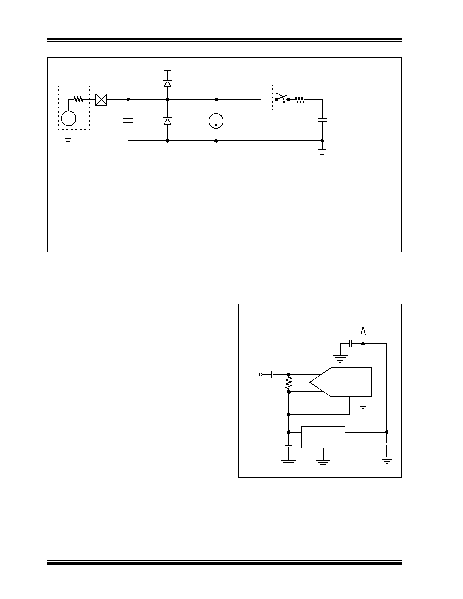
FIGURE 5-3:
Analog Input Model.
5.2.1
MAINTAINING MINIMUM CLOCK
SPEED
When the MCP3302/04 initiates, charge is stored on
the sample capacitor. When the sample period is
complete, the device converts one bit for each clock
that is received. It is important for the user to note that
a slow clock rate will allow charge to bleed off the
sample capacitor while the conversion is taking place.
For the MCP330X devices, the recommended mini-
mum clock speed during the conversion cycle (TCONV)
is 105 kHz. Failure to meet this criteria may induce
linearity errors into the conversion outside the rated
specifications. It should be noted that during the entire
conversion cycle, the A/D converter does not have
requirements for clock speed or duty cycle, as long as
all timing specifications are met.
5.3
Biasing Solutions
For pseudo-differential bipolar operation, the biasing
circuit shown in Figure 5-4 shows a single-ended input
AC coupled to the converter. This configuration will give
a digital output range of -4096 to +4095. With the 2.5V
reference, the LSB size equal to 610 V.
Although the ADC is not production tested with a 2.5V
reference as shown, linearity will not change more than
0.1 LSB. See Figure 2-2 and Figure 2-6 for INL and
DNL errors versus V
REF at V
DD = 5V. A trade-off exists
between the high-pass corner and the acquisition time.
The value of C will need to be quite large in order to
bring down the high-pass corner. The value of R needs
to be 1 k, or less, since higher input impedances
require additional acquisition time.
Using the values in Figure 5-4, we have a 100 Hz cor-
ner frequency. See Figure 5-2 for relation between
input impedance and acquisition time.
FIGURE 5-4:
Pseudo-differential biasing
circuit for bipolar operation.
CPIN
VA
RS
CHx
7pF
VT = 0.6V
ILEAKAGE
Sampling
Switch
SS
RSS = 1 k
CSAMPLE
= DAC capacitance
VSS
VDD
= 25 pF
±1 nA
Legend
VA = signal source
RS = source impedance
CHx = input channel pad
CPIN = input pin capacitance
VT = threshold voltage
ILEAKAGE = leakage current at the pindue to various junctions
SS = sampling switch
RSS = sampling switch resistor
CSAMPLE = sample/hold capacitance
VDD = 5V
0.1 F
IN+
IN-
VREF
MCP330X
1F
MCP1525
VIN
VOUT
0.1 F
1k
10 F
VIN
R
C
相关PDF资料 |
PDF描述 |
|---|---|
| NCP2890DMR2G | IC AMP POWER AUDIO 1W 8MICRO |
| VE-263-IV-B1 | CONVERTER MOD DC/DC 24V 150W |
| VE-262-IV-B1 | CONVERTER MOD DC/DC 15V 150W |
| MAX9722AETE+T | IC AMP AUDIO .13W STER AB 16TQFN |
| 17291-3PG-3ES | CONN RCPT 3POS PNL MNT PIN |
相关代理商/技术参数 |
参数描述 |
|---|---|
| MCP3304TI/P | 制造商:MICROCHIP 制造商全称:Microchip Technology 功能描述:13-Bit Differential Input, Low Power A/D Converter with SPI Serial Interface |
| MCP3304T-I/P | 制造商:MICROCHIP 制造商全称:Microchip Technology 功能描述:13-Bit Differential Input, Low Power A/D Converter with SPI Serial Interface |
| MCP3304TI/SL | 制造商:MICROCHIP 制造商全称:Microchip Technology 功能描述:13-Bit Differential Input, Low Power A/D Converter with SPI Serial Interface |
| MCP3304T-I/SL | 制造商:MICROCHIP 制造商全称:Microchip Technology 功能描述:13-Bit Differential Input, Low Power A/D Converter with SPI Serial Interface |
| MCP3304TI/ST | 制造商:MICROCHIP 制造商全称:Microchip Technology 功能描述:13-Bit Differential Input, Low Power A/D Converter with SPI Serial Interface |
发布紧急采购,3分钟左右您将得到回复。