参数资料
| 型号: | MCP631T-E/MNY |
| 厂商: | Microchip Technology |
| 文件页数: | 14/62页 |
| 文件大小: | 0K |
| 描述: | IC OP AMP SGL 24MHZ 8-TDFN |
| 标准包装: | 3,300 |
| 放大器类型: | 通用 |
| 电路数: | 1 |
| 输出类型: | 满摆幅 |
| 转换速率: | 10 V/µs |
| 增益带宽积: | 24MHz |
| 电流 - 输入偏压: | 4pA |
| 电压 - 输入偏移: | 1800µV |
| 电流 - 电源: | 2.5mA |
| 电流 - 输出 / 通道: | 70mA |
| 电压 - 电源,单路/双路(±): | 2.5 V ~ 5.5 V |
| 工作温度: | -40°C ~ 125°C |
| 安装类型: | 表面贴装 |
| 封装/外壳: | 8-WFDFN 裸露焊盘 |
| 供应商设备封装: | 8-TDFN(2x3) |
| 包装: | 带卷 (TR) |
第1页第2页第3页第4页第5页第6页第7页第8页第9页第10页第11页第12页第13页当前第14页第15页第16页第17页第18页第19页第20页第21页第22页第23页第24页第25页第26页第27页第28页第29页第30页第31页第32页第33页第34页第35页第36页第37页第38页第39页第40页第41页第42页第43页第44页第45页第46页第47页第48页第49页第50页第51页第52页第53页第54页第55页第56页第57页第58页第59页第60页第61页第62页
2009-2011 Microchip Technology Inc.
DS22197B-page 21
MCP631/2/3/4/5/9
4.0
APPLICATIONS
The MCP631/2/3/4/5/9 family op amps is manufactured
using the Microchip state-of-the-art CMOS process. It
is designed for low cost, low power and high speed
applications. Its low supply voltage, low quiescent
current and wide bandwidth make the MCP631/2/3/4/5/
9 ideal for battery-powered applications.
4.1
Input
4.1.1
PHASE REVERSAL
The input devices are designed to not exhibit phase
inversion when the input pins exceed the supply
voltages.
Figure 2-38 shows
an
input voltage
exceeding both supplies with no phase inversion.
4.1.2
INPUT VOLTAGE AND CURRENT
LIMITS
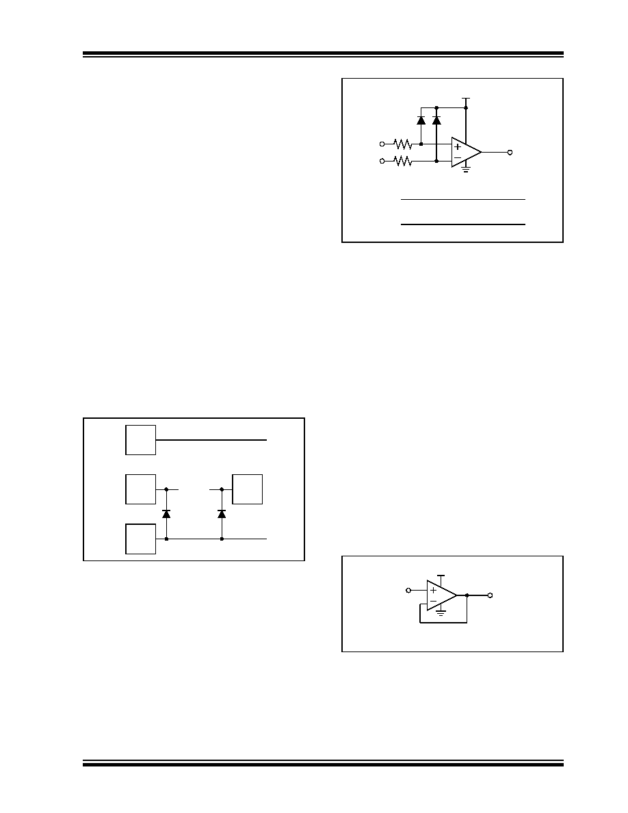
The electrostatic discharge (ESD) protection on the
inputs can be depicted as shown in Figure 4-1. This
structure was chosen to protect the input transistors,
and to minimize input bias current (IB). The input ESD
diodes clamp the inputs when they try to go more than
one diode drop below VSS. They also clamp any volt-
ages that go too far above VDD; their breakdown volt-
age is high enough to allow normal operation, and low
enough to bypass quick ESD events within the speci-
fied limits.
FIGURE 4-1:
Simplified Analog Input ESD
Structures.
In order to prevent damage and/or improper operation
of these amplifiers, the circuit must limit the currents
(and voltages) at the input pins (see Section 1.1
the recommended approach to protecting these inputs.
The internal ESD diodes prevent the input pins
(VIN+and VIN-) from going too far below ground, and
the resistors R1 and R2 limit the possible current drawn
out of the input pins. Diodes D1 and D2 prevent the
input pins (VIN+ and VIN-) from going too far above
VDD, and dump any currents onto VDD. When
implemented as shown, resistors R1 and R2 also limit
the current through D1 and D2.
FIGURE 4-2:
Protecting the Analog
Inputs.
It is also possible to connect the diodes to the left of the
resistor R1 and R2. In this case, the currents through
the diodes D1 and D2 need to be limited by some other
mechanism. The resistors then serve as in-rush
current limiters; the DC current into the input pins
(VIN+ and VIN-) should be very small.
A significant amount of current can flow out of the
inputs (through the ESD diodes) when the common
mode voltage (VCM) is below ground (VSS); see
Figure 2-13. Applications that are high-impedance may
need to limit the usable voltage range.
4.1.3
NORMAL OPERATION
The input stage of the MCP631/2/3/4/5/9 op amps uses
a differential PMOS input stage. It operates at
low common mode input voltages (VCM), with VCM
between VSS – 0.3V and VDD – 1.3V. To ensure proper
operation, the input offset voltage (VOS) is measured
at both
VCM =VSS – 0.3V
and
VDD –1.3V.
See Figure 2-5 and Figure 2-6 for temperature effects.
When operating at very low non-inverting gains, the
output voltage is limited at the top by the VCM range
FIGURE 4-3:
Unity Gain Voltage
Limitations for Linear Operation.
Bond
Pad
Bond
Pad
Bond
Pad
VDD
VIN+
VSS
Input
Stage
Bond
Pad
VIN-
V1
R1
VDD
D1
R1 >
VSS – (minimum expected V1)
2mA
VOUT
R2 >
VSS – (minimum expected V2)
2mA
V2
R2
D2
MCP63X
VIN
VDD
VOUT
VSS V
IN V
OUT
VDD 1.3V
–
MCP63X
相关PDF资料 |
PDF描述 |
|---|---|
| MCP631T-E/SN | IC OPAMP R-R 24MHZ 8SOIC |
| TLV342IDG4 | IC OPAMP GP R-R 2.3MHZ 8SOIC |
| 2510-6003UB | CONN HEADER 10POS STR GOLD T/H |
| FWJ-08-01-T-S | CONN HEADER .156" 8POS SNGL TIN |
| 68602-572 | BERGSTIK II .100" DR STRAIGHT |
相关代理商/技术参数 |
参数描述 |
|---|---|
| MCP632-E/MF | 功能描述:运算放大器 - 运放 Dual 24MHz OP E temp RoHS:否 制造商:STMicroelectronics 通道数量:4 共模抑制比(最小值):63 dB 输入补偿电压:1 mV 输入偏流(最大值):10 pA 工作电源电压:2.7 V to 5.5 V 安装风格:SMD/SMT 封装 / 箱体:QFN-16 转换速度:0.89 V/us 关闭:No 输出电流:55 mA 最大工作温度:+ 125 C 封装:Reel |
| MCP632-E/SN | 功能描述:运算放大器 - 运放 Dual 24MHz OP E temp RoHS:否 制造商:STMicroelectronics 通道数量:4 共模抑制比(最小值):63 dB 输入补偿电压:1 mV 输入偏流(最大值):10 pA 工作电源电压:2.7 V to 5.5 V 安装风格:SMD/SMT 封装 / 箱体:QFN-16 转换速度:0.89 V/us 关闭:No 输出电流:55 mA 最大工作温度:+ 125 C 封装:Reel |
| MCP632T-E/MF | 功能描述:运算放大器 - 运放 Dual 24MHz OP E temp RoHS:否 制造商:STMicroelectronics 通道数量:4 共模抑制比(最小值):63 dB 输入补偿电压:1 mV 输入偏流(最大值):10 pA 工作电源电压:2.7 V to 5.5 V 安装风格:SMD/SMT 封装 / 箱体:QFN-16 转换速度:0.89 V/us 关闭:No 输出电流:55 mA 最大工作温度:+ 125 C 封装:Reel |
| MCP632T-E/SN | 功能描述:运算放大器 - 运放 Dual 24MHz OP E temp RoHS:否 制造商:STMicroelectronics 通道数量:4 共模抑制比(最小值):63 dB 输入补偿电压:1 mV 输入偏流(最大值):10 pA 工作电源电压:2.7 V to 5.5 V 安装风格:SMD/SMT 封装 / 箱体:QFN-16 转换速度:0.89 V/us 关闭:No 输出电流:55 mA 最大工作温度:+ 125 C 封装:Reel |
| MCP633-E/SN | 功能描述:运算放大器 - 运放 Single 24MHz OP w /CS E temp RoHS:否 制造商:STMicroelectronics 通道数量:4 共模抑制比(最小值):63 dB 输入补偿电压:1 mV 输入偏流(最大值):10 pA 工作电源电压:2.7 V to 5.5 V 安装风格:SMD/SMT 封装 / 箱体:QFN-16 转换速度:0.89 V/us 关闭:No 输出电流:55 mA 最大工作温度:+ 125 C 封装:Reel |
发布紧急采购,3分钟左右您将得到回复。