- 您现在的位置:买卖IC网 > PDF目录3405 > MCP6N11T-005E/SN (Microchip Technology)IC AMP INSTR RRIO 2.5MHZ 8SOIC PDF资料下载
参数资料
| 型号: | MCP6N11T-005E/SN |
| 厂商: | Microchip Technology |
| 文件页数: | 20/50页 |
| 文件大小: | 0K |
| 描述: | IC AMP INSTR RRIO 2.5MHZ 8SOIC |
| 标准包装: | 3,300 |
| 放大器类型: | 仪表 |
| 电路数: | 1 |
| 输出类型: | 满摆幅 |
| 转换速率: | 9 V/µs |
| 增益带宽积: | 2.5MHz |
| 电流 - 输入偏压: | 10pA |
| 电压 - 输入偏移: | 850µV |
| 电流 - 电源: | 800µA |
| 电流 - 输出 / 通道: | 30mA |
| 电压 - 电源,单路/双路(±): | 1.8 V ~ 5.5 V |
| 工作温度: | -40°C ~ 125°C |
| 安装类型: | 表面贴装 |
| 封装/外壳: | 8-SOIC(0.154",3.90mm 宽) |
| 供应商设备封装: | 8-SOICN |
| 包装: | 带卷 (TR) |
第1页第2页第3页第4页第5页第6页第7页第8页第9页第10页第11页第12页第13页第14页第15页第16页第17页第18页第19页当前第20页第21页第22页第23页第24页第25页第26页第27页第28页第29页第30页第31页第32页第33页第34页第35页第36页第37页第38页第39页第40页第41页第42页第43页第44页第45页第46页第47页第48页第49页第50页
2011 Microchip Technology Inc.
DS25073A-page 27
MCP6N11
4.0
APPLICATIONS
The MCP6N11 instrumentation amplifier (INA) is
manufactured using Microchip’s state of the art CMOS
process. It is low cost, low power and high speed,
making it ideal for battery-powered applications.
4.1
Basic Performance
4.1.1
STANDARD CIRCUIT
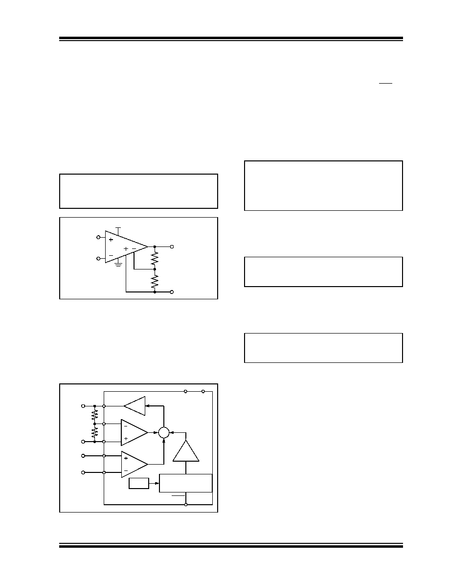
Figure 4-1 shows the standard circuit configuration for
these INAs. When the inputs and output are in their
specified ranges, the output voltage is approximately:
EQUATION 4-1:
FIGURE 4-1:
Standard Circuit.
For normal operation, keep:
VIP, VIM, VREF and VFG between VIVL and VIVH
VIP – VIM (i.e., VDM) between VDML and VDMH
VOUT between VOL and VOH
4.1.2
ARCHITECTURE
Figure 4-2 shows the block diagram for these INAs.
FIGURE 4-2:
MCP6N11 Block Diagram.
The input offset voltage (VOS) is corrected by the
voltage VTR. Each time a VOS Calibration event occurs,
VTR is updated to the best value (at that moment).
These events are triggered by either powering up
(monitored by the POR) or by toggling the EN/CAL pin
high. The current out of GM3 (I3) is constant and very
small (assumed to be zero in the following discussion).
the relationships between the input voltages (VIP and
VIM) and the common mode and differential voltages
(VCM and VDM).
EQUATION 4-2:
The negative feedback loop includes GM2, RM4, RF and
RG. These blocks set the DC open-loop gain (AOL) and
the nominal differential gain (GDM):
EQUATION 4-3:
AOL is very high, so I4 is very small and I1 + I2 ≈ 0. This
makes the differential inputs to GM1 and GM2 equal in
magnitude and opposite in polarity. Ideally, this gives:
EQUATION 4-4:
For an ideal part, changing VCM, VSS or VDD produces
no change in VOUT. VREF shifts VOUT as needed.
The different GMIN options change GM1, GM2 and the
internal compensation capacitor. This results in the
performance trade-offs shown in Table 1.
VOUT ≈ VREF +GDMVDM
Where:
GDM =1 +RF /RG
VOUT
VIP
VDD
VIM
VREF
VFG
RF
RG
U1
MCP6N11
RF
VFG
VOUT
Low Power
VSS
VDD
EN/CAL
VOUT
VOS Calibration
VREF
RM4
GM2
Σ
I2
VREF
I4
GM3
I3
VTR
RG
VIP
VIM
GM1
I1
VIP
VIM
POR
V
IP
V
CM
V
DM 2
+
=
V
IM
V
CM
V
DM 2
–
=
V
CM
V
IP
V
IM
+
() 2
=
V
DM
V
IP
V
IM
–
=
A
OL
G
M2RM4
=
G
DM
1R
F RG
+
=
V
FG
V
REF
–
()
V
DM
=
V
OUT
V
DMGDM
V
REF
+
=
相关PDF资料 |
PDF描述 |
|---|---|
| P6KE400CA-HF | TVS 600W 400V BIDIRECT DO-15 |
| 76382-404 | CONN HEADER 4POS .100" R/A TIN |
| 76383-309 | CONN HEADER 18PS.100 DL R/A GOLD |
| PCN10C-44S-2.54DS | DIN CONN RCPT 44 POS 2 ROW R ANG |
| MCP6N11T-002E/SN | IC AMP INSTR RRIO 1MHZ 8SOIC |
相关代理商/技术参数 |
参数描述 |
|---|---|
| MCP6N11T-010E/MNY | 功能描述:仪表放大器 Sngl Instrumentation Amp mCal E temp RoHS:否 制造商:Texas Instruments 通道数量: 输入补偿电压:150 V 可用增益调整: 最大输入电阻:10 kOhms 共模抑制比(最小值):88 dB 工作电源电压:2.7 V to 36 V 电源电流:200 uA 最大工作温度:+ 125 C 最小工作温度:- 40 C 封装 / 箱体:MSOP-8 封装:Bulk |
| MCP6N11T-010E/SN | 功能描述:仪表放大器 Sngl Instrumentation Amp mCal E temp RoHS:否 制造商:Texas Instruments 通道数量: 输入补偿电压:150 V 可用增益调整: 最大输入电阻:10 kOhms 共模抑制比(最小值):88 dB 工作电源电压:2.7 V to 36 V 电源电流:200 uA 最大工作温度:+ 125 C 最小工作温度:- 40 C 封装 / 箱体:MSOP-8 封装:Bulk |
| MCP6N11T-100E/MNY | 功能描述:仪表放大器 Sngl Instrumentation Amp mCal E temp RoHS:否 制造商:Texas Instruments 通道数量: 输入补偿电压:150 V 可用增益调整: 最大输入电阻:10 kOhms 共模抑制比(最小值):88 dB 工作电源电压:2.7 V to 36 V 电源电流:200 uA 最大工作温度:+ 125 C 最小工作温度:- 40 C 封装 / 箱体:MSOP-8 封装:Bulk |
| MCP6N11T-100E/SN | 功能描述:仪表放大器 Sngl Instrumentation Amp mCal E temp RoHS:否 制造商:Texas Instruments 通道数量: 输入补偿电压:150 V 可用增益调整: 最大输入电阻:10 kOhms 共模抑制比(最小值):88 dB 工作电源电压:2.7 V to 36 V 电源电流:200 uA 最大工作温度:+ 125 C 最小工作温度:- 40 C 封装 / 箱体:MSOP-8 封装:Bulk |
| MCP6S21-I/MS | 功能描述:特殊用途放大器 1-Chan. 12 MHz SPI RoHS:否 制造商:Texas Instruments 通道数量:Single 共模抑制比(最小值): 输入补偿电压: 工作电源电压:3 V to 5.5 V 电源电流:5 mA 最大功率耗散: 最大工作温度:+ 70 C 最小工作温度:- 40 C 安装风格:SMD/SMT 封装 / 箱体:QFN-20 封装:Reel |
发布紧急采购,3分钟左右您将得到回复。