参数资料
| 型号: | MCP6V28T-E/MS |
| 厂商: | Microchip Technology |
| 文件页数: | 18/50页 |
| 文件大小: | 0K |
| 描述: | IC OPAMP AUTO-ZERO SGL 8SOIC |
| 标准包装: | 2,500 |
| 放大器类型: | 自动调零 |
| 电路数: | 1 |
| 输出类型: | 满摆幅 |
| 转换速率: | 1 V/µs |
| 增益带宽积: | 2MHz |
| 电流 - 输入偏压: | 7pA |
| 电压 - 输入偏移: | 2µV |
| 电流 - 电源: | 620µA |
| 电流 - 输出 / 通道: | 22mA |
| 电压 - 电源,单路/双路(±): | 2.3 V ~ 5.5 V |
| 工作温度: | -40°C ~ 125°C |
| 安装类型: | 表面贴装 |
| 封装/外壳: | 8-TSSOP,8-MSOP(0.118",3.00mm 宽) |
| 供应商设备封装: | 8-MSOP |
| 包装: | 带卷 (TR) |
第1页第2页第3页第4页第5页第6页第7页第8页第9页第10页第11页第12页第13页第14页第15页第16页第17页当前第18页第19页第20页第21页第22页第23页第24页第25页第26页第27页第28页第29页第30页第31页第32页第33页第34页第35页第36页第37页第38页第39页第40页第41页第42页第43页第44页第45页第46页第47页第48页第49页第50页
2011 Microchip Technology Inc.
DS25007B-page 25
MCP6V26/7/8
4.3.6
CAPACITIVE LOADS
Driving large capacitive loads can cause stability
problems for voltage feedback op amps. As the load
capacitance increases, the feedback loop’s phase
margin decreases and the closed-loop bandwidth is
reduced. This produces gain peaking in the frequency
response, with overshoot and ringing in the step
response. These auto-zeroed op amps have a different
output impedance than most op amps, due to their
unique topology.
When driving a capacitive load with these op amps, a
improves the feedback loop’s phase margin (stability)
by making the output load resistive at higher
frequencies. The bandwidth will be generally lower
than the bandwidth with no capacitive load.
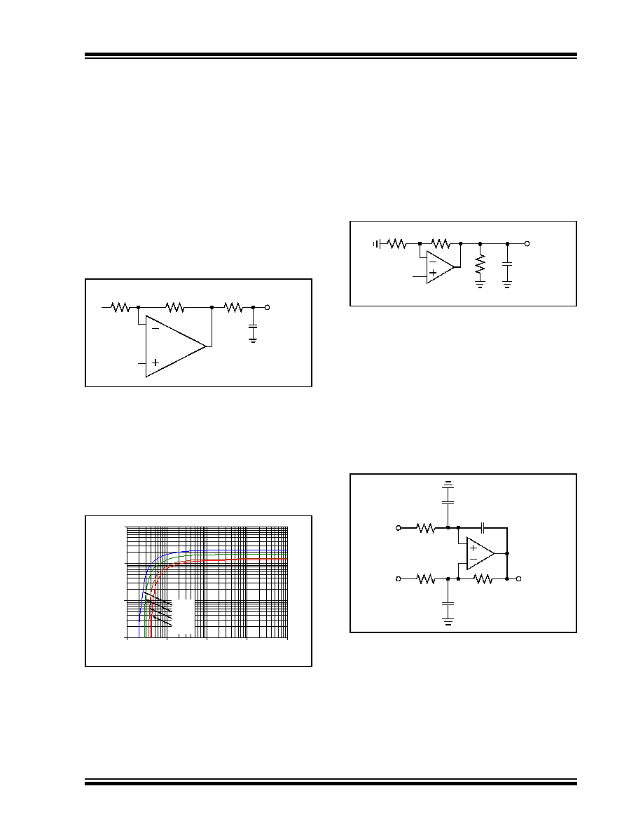
FIGURE 4-7:
Output Resistor, RISO,
Stabilizes Capacitive Loads.
different capacitive loads and gains. The x-axis is the
normalized load capacitance (CL/GN2). The y-axis is
the normalized resistance (GNRISO).
GN is the circuit’s noise gain. For non-inverting gains,
GN and the Signal Gain are equal. For inverting gains,
GN is 1+|Signal Gain| (e.g., -1 V/V gives GN = +2 V/V).
FIGURE 4-8:
Recommended RISO values
for Capacitive Loads.
After selecting RISO for your circuit, double check the
resulting frequency response peaking and step
response overshoot. Modify RISO's value until the
response is reasonable. Bench evaluation and
simulations with the MCP6V26/7/8 SPICE macro
model are helpful.
4.3.7
STABILIZING OUTPUT LOADS
This family of auto-zeroed op amps has an output
impedance (Figure 2-31 and Figure 2-32) that has a
double zero when the gain is low. This can cause a
large phase shift in feedback networks that have low
resistance near the part’s bandwidth. This large phase
shift can cause stability problems.
Figure 4-9 shows that the load on the output is
(RL +RISO)||(RF +RG), where RISO is before the load
(like Figure 4-7). This load needs to be large enough to
maintain stability; it should be at least (2 k
Ω)/GN.
FIGURE 4-9:
Output Load.
4.3.8
GAIN PEAKING
Figure 4-10 shows an op amp circuit that represents
non-inverting amplifiers (VM is a DC voltage and VP is
the input) or inverting amplifiers (VP is a DC voltage
and VM is the input). The capacitances CN and CG rep-
resent the total capacitance at the input pins; they
include the op amp’s common mode input capacitance
(CCM), board parasitic capacitance and any capacitor
placed in parallel. The capacitance CFP represents the
parasitic capacitance coupling the output and
non-inverting input pins.
FIGURE 4-10:
Amplifier with Parasitic
Capacitance.
CG acts in parallel with RG (except for a gain of +1 V/V),
which causes an increase in gain at high frequencies.
CG also reduces the phase margin of the feedback
loop, which becomes less stable. This effect can be
reduced by either reducing CG or RF||RG.
CN and RN form a low-pass filter that affects the signal
at VP. This filter has a single real pole at 1/(2πRNCN).
RISO
CL
VOUT
U1
MCP6V2X
1
10
100
1000
1.E-10
1.E-09
1.E-08
1.E-07
1.E-06
CL/GN
2 (F)
Recommended
G
N
R
ISO
()
100p
1n
10n
100n
1μ
1
10
100
1k
GN = 1
GN = 2
GN = 5
GN 10
RG
RF
VOUT
RL
CL
U1
MCP6V2X
RF
CG
RN
VOUT
U1
MCP6V2X
RG
VM
VP
CFP
CN
相关PDF资料 |
PDF描述 |
|---|---|
| EL5161IWZ-T7 | IC AMP CFA SGL 200MHZ SOT23-5 |
| MTLW-107-05-G-D-170 | CONN HEADER 14POS 1.00" DL GOLD |
| TSW-108-07-G-T | CONN HEADER 24POS .100" AU |
| 3429-6002UG | CONN HEADER 26POS STR NO LATCH |
| TST-108-04-L-D-RA | CONN HEADER 16POS .100" R/A GOLD |
相关代理商/技术参数 |
参数描述 |
|---|---|
| MCP6V31T-E/OT | 功能描述:运算放大器 - 运放 Single, Zero Drift Op Amp, E Temp RoHS:否 制造商:STMicroelectronics 通道数量:4 共模抑制比(最小值):63 dB 输入补偿电压:1 mV 输入偏流(最大值):10 pA 工作电源电压:2.7 V to 5.5 V 安装风格:SMD/SMT 封装 / 箱体:QFN-16 转换速度:0.89 V/us 关闭:No 输出电流:55 mA 最大工作温度:+ 125 C 封装:Reel |
| MCP6V31T-E/OT-CUT TAPE | 制造商:Microchip Technology 功能描述:Cut Tape 制造商:Microchip Technology 功能描述:SP Amp Zero Drift Amplifier Single R-R I/O 5.5V 5-Pin SOT-23 T/R |
| MCP6V31UT-E/LT | 功能描述:运算放大器 - 运放 Single, Zero Drift Op Amp, E Temp RoHS:否 制造商:STMicroelectronics 通道数量:4 共模抑制比(最小值):63 dB 输入补偿电压:1 mV 输入偏流(最大值):10 pA 工作电源电压:2.7 V to 5.5 V 安装风格:SMD/SMT 封装 / 箱体:QFN-16 转换速度:0.89 V/us 关闭:No 输出电流:55 mA 最大工作温度:+ 125 C 封装:Reel |
| MCP6V31UT-E/OT | 功能描述:运算放大器 - 运放 Single, Zero Drift Op Amp, E Temp RoHS:否 制造商:STMicroelectronics 通道数量:4 共模抑制比(最小值):63 dB 输入补偿电压:1 mV 输入偏流(最大值):10 pA 工作电源电压:2.7 V to 5.5 V 安装风格:SMD/SMT 封装 / 箱体:QFN-16 转换速度:0.89 V/us 关闭:No 输出电流:55 mA 最大工作温度:+ 125 C 封装:Reel |
| MCP6V31UT-E/OT-CUT TAPE | 制造商:Microchip Technology 功能描述:Cut Tape 制造商:Microchip Technology 功能描述:SP Amp Zero Drift Amplifier Single R-R I/O 5.5V 5-Pin SOT-23 T/R |
发布紧急采购,3分钟左右您将得到回复。