- 您现在的位置:买卖IC网 > PDF目录9430 > MCP795W10-I/ST (Microchip Technology)IC RTCC 64B SRAM WD/DET 14TSSOP PDF资料下载
参数资料
| 型号: | MCP795W10-I/ST |
| 厂商: | Microchip Technology |
| 文件页数: | 5/13页 |
| 文件大小: | 0K |
| 描述: | IC RTCC 64B SRAM WD/DET 14TSSOP |
| 标准包装: | 96 |
| 类型: | 时钟/日历 |
| 特点: | 警报,EEPROM,闰年,方波输出,SRAM,看门狗定时器 |
| 存储容量: | 64B |
| 时间格式: | HH:MM:SS:hh(12/24 小时) |
| 数据格式: | YY-MM-DD-dd |
| 接口: | SPI |
| 电源电压: | 1.8 V ~ 5.5 V |
| 电压 - 电源,电池: | 1.3 V ~ 5.5 V |
| 工作温度: | -40°C ~ 85°C |
| 安装类型: | 表面贴装 |
| 封装/外壳: | 14-TSSOP(0.173",4.40mm 宽) |
| 供应商设备封装: | 14-TSSOP |
| 包装: | 管件 |
MCP4902/4912/4922
DS22250A-page 28
2010 Microchip Technology Inc.
6.4
Single-Supply Operation
The MCP4902/4912/4922 family of devices are rail-to-
rail voltage output DAC devices designed to operate
with a VDD range of 2.7V to 5.5V. Its output amplifier is
robust enough to drive small-signal loads directly.
Therefore, it does not require any external output buffer
for most applications.
6.4.1
DC SET POINT OR CALIBRATION
A common application for the DAC devices is
digitally-controlled set points and/or calibration of
variable parameters, such as sensor offset or slope.
For example, the MCP4922 provides 4096 output
steps. If the external voltage reference (VREF) is
4.096V, the LSb size is 1 mV. If a smaller output step
size is desired, a lower external voltage reference is
needed.
6.4.1.1
Decreasing Output Step Size
If the application is calibrating the bias voltage of a
diode or transistor, a bias voltage range of 0.8V may be
desired with about 200 V resolution per step. Two
common methods to achieve a 0.8V range is to either
reduce VREF to 0.82V or use a voltage divider on the
DAC’s output.
Using a VREF is an option if the VREF is available with
the
desired
output
voltage
range.
However,
occasionally, when using a low-voltage VREF, the noise
floor causes SNR error that is intolerable. Using a
voltage divider method is another option and provides
some advantages when VREF needs to be very low or
when the desired output voltage is not available. In this
case, a larger value VREF is used while two resistors
scale the output range down to the precise desired
level.
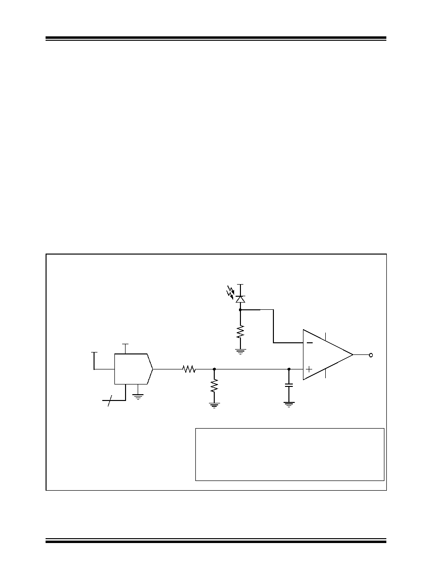
Example 6-1 illustrates this concept. Note that the
bypass capacitor on the output of the voltage divider
plays a critical function in attenuating the output noise
of the DAC and the induced noise from the
environment.
EXAMPLE 6-1:
EXAMPLE CIRCUIT OF SET POINT OR THRESHOLD CALIBRATION
VDD
SPI
3-wire
VTRIP
R1
R2
0.1 uF
Comparator
G = Gain selection (1x or 2x)
Dn = Digital value of DAC (0-255) for MCP4901/MCP4902
VOUT
VREF G
Dn
2
N
------
=
VCC+
VCC–
VOUT
Vtrip
VOUT
R2
R1 R2
+
--------------------
=
VDD
RSENSE
DAC
= Digital value of DAC (0-1023) for MCP4911/MCP4912
= Digital value of DAC (0-4095) for MCP4921/MCP4922
N = DAC Bit Resolution
VREF
VO
MCP4901
MCP4911
MCP4921
(a) Single Output DAC:
(b) Dual Output DAC:
MCP4902
MCP4912
MCP4922
相关PDF资料 |
PDF描述 |
|---|---|
| AD5243BRMZ100 | IC DGTL POT DUAL 100K I2C 10MSOP |
| MCP795W10-I/SL | IC RTCC 64B SRAM WD/DET 14SOIC |
| AD5248BRMZ50 | IC DGTL POT DUAL 50K I2C 10-MSOP |
| AD5162BRMZ10 | IC POT DUAL 10K 256POS 10-MSOP |
| AD5248BRMZ10 | IC DGTL POT DUAL 10K I2C 10-MSOP |
相关代理商/技术参数 |
参数描述 |
|---|---|
| MCP795W10T-I/SL | 功能描述:实时时钟 1Kb EE 64B SRAM WD TED ID RoHS:否 制造商:Microchip Technology 功能:Clock, Calendar. Alarm RTC 总线接口:I2C 日期格式:DW:DM:M:Y 时间格式:HH:MM:SS RTC 存储容量:64 B 电源电压-最大:5.5 V 电源电压-最小:1.8 V 最大工作温度:+ 85 C 最小工作温度: 安装风格:Through Hole 封装 / 箱体:PDIP-8 封装:Tube |
| MCP795W10T-I/ST | 功能描述:实时时钟 1Kb EE 64B SRAM WD TED ID RoHS:否 制造商:Microchip Technology 功能:Clock, Calendar. Alarm RTC 总线接口:I2C 日期格式:DW:DM:M:Y 时间格式:HH:MM:SS RTC 存储容量:64 B 电源电压-最大:5.5 V 电源电压-最小:1.8 V 最大工作温度:+ 85 C 最小工作温度: 安装风格:Through Hole 封装 / 箱体:PDIP-8 封装:Tube |
| MCP795W11 | 制造商:MAS 制造商全称:MAS 功能描述:SPI Real-Time Clock Calendar |
| MCP795W11-I/SL | 功能描述:实时时钟 1Kb EE 64B SRAM WD TED EUI-48 RoHS:否 制造商:Microchip Technology 功能:Clock, Calendar. Alarm RTC 总线接口:I2C 日期格式:DW:DM:M:Y 时间格式:HH:MM:SS RTC 存储容量:64 B 电源电压-最大:5.5 V 电源电压-最小:1.8 V 最大工作温度:+ 85 C 最小工作温度: 安装风格:Through Hole 封装 / 箱体:PDIP-8 封装:Tube |
| MCP795W11-I/ST | 功能描述:实时时钟 1Kb EE 64B SRAM WD TED EUI-48 RoHS:否 制造商:Microchip Technology 功能:Clock, Calendar. Alarm RTC 总线接口:I2C 日期格式:DW:DM:M:Y 时间格式:HH:MM:SS RTC 存储容量:64 B 电源电压-最大:5.5 V 电源电压-最小:1.8 V 最大工作温度:+ 85 C 最小工作温度: 安装风格:Through Hole 封装 / 箱体:PDIP-8 封装:Tube |
发布紧急采购,3分钟左右您将得到回复。