- 您现在的位置:买卖IC网 > PDF目录13131 > MIC9130YQS (Micrel Inc)IC CTRLR DC-DC PWM HV HS 16-QSOP PDF资料下载
参数资料
| 型号: | MIC9130YQS |
| 厂商: | Micrel Inc |
| 文件页数: | 10/19页 |
| 文件大小: | 0K |
| 描述: | IC CTRLR DC-DC PWM HV HS 16-QSOP |
| 标准包装: | 98 |
| 应用: | 控制器,电信 |
| 输入电压: | 9 V ~ 18 V |
| 输出数: | 1 |
| 输出电压: | 4.7 V ~ 5 V |
| 工作温度: | -40°C ~ 125°C |
| 安装类型: | 表面贴装 |
| 封装/外壳: | 16-SSOP(0.154",3.90mm 宽) |
| 供应商设备封装: | 16-QSOP |
| 包装: | 管件 |
| 产品目录页面: | 1086 (CN2011-ZH PDF) |
| 其它名称: | 576-2418 MIC9130YQS-ND |
�� �
�
�MIC9130�
�Start-up� circuit� operation� is� illustrated� in� Figure� 2.� V� IN� is� ap-�
�plied� and� the� depletion� FET,� which� is� normally� enabled� allows�
�current� from� V� IN� to� charge� the� V� CC� bias� capacitor.� Once� the�
�V� CC� voltage� reaches� the� V� CC� enable� threshold,� V� GLO� (ON)� ,�
�the� gate� drive� is� enabled� and� the� MIC9130� starts� switching.�
�V� CC� continues� to� increase� until� the� Pre-Regulator� turn-off�
�threshold,� (V� PR� (OFF)),� is� reached� and� the� depletion� FET� is�
�turned� off.� The� V� CC� voltage� decreases� as� energy� from� the�
�bias� capacitor� is� used� to� supply� the� controller.� The� deple-�
�tion� FET� is� turned� back� on� when� the� pre-regulator� turn-on�
�threshold� is� reached.� A� bias� winding� derived� supply� voltage,�
�set� higher� than� the� FET� turn-off� threshold,� V� PR� (OFF),� raises�
�the� V� CC� voltage� over� the� threshold� and� prevents� the� FET�
�from� turning� on.�
�In� certain� designs� the� MIC9130� may� be� powered� directly� from�
�the� Line� voltage,� eliminating� the� need� for� an� extra� transformer�
�bias� winding.� When� operating� in� this� fashion� the� designer�
�must� insure� the� power� dissipation� in� the� IC� does� not� cause�
�the� die� temperature� to� exceed� the� 125°C� maximum.� Power�
�dissipation� is� calculated� by:�
�P� DISS� =� (� V� IN� ?� V� CC� )� � I� VCC�
�Where� :�
�V� IN� is� the� line� input� voltage�
�V� CC� is� the� average� V� CC� voltage� (typically� 8.5V)�
�I� VCC� is� the� total� current� drawn� by� the� IC�
�I� VCC� is� the� sum� of� the� operating� current� of� the� MIC9130� at�
�a� given� frequency� and� the� average� current� required� to� drive�
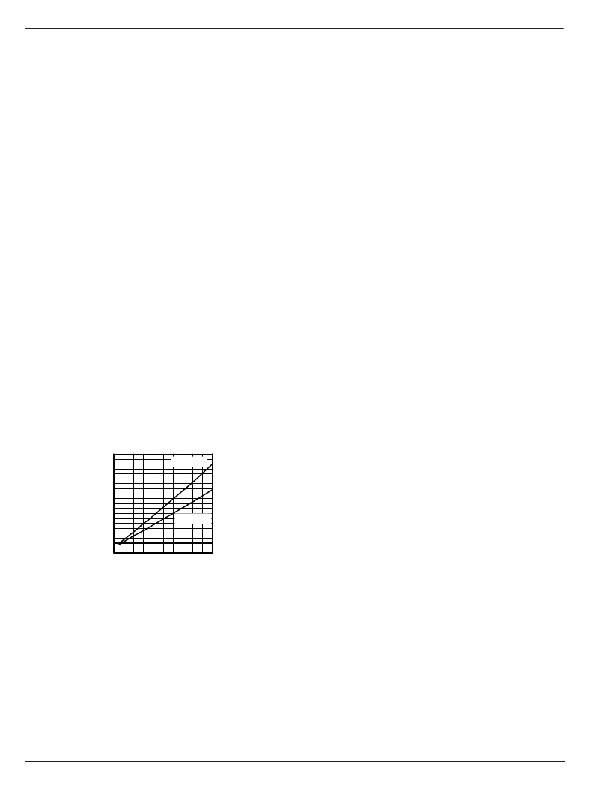
�the� external� switching� MOSFET.� A� plot� of� typical� operating�
�current� vs.� frequency� is� given� in� Figure� 3.� The� average� MOS-�
�FET� gate� drive� current� is� calculated� in� the� “MOSFET� GATE�
�DRIVE”� section� of� this� speci� ?� cation.�
�Micrel,� Inc.�
�for� most� topologies� since� the� variation� is� small� (equal� to� the�
�Δ� V� PR� hysteresis).� The� bias� regulator� in� the� MIC9130� buffers�
�the� internal� circuits� from� V� CC� variations.�
�The� pre-regulator� FET� is� protected� by� a� thermal� shutdown�
�circuit,� which� turns� the� MOSFET� off� if� its� temperature� exceeds�
�approximately� 150� degrees� C.�
�When� operating� at� input� voltages� greater� than� 150V,� a� fast�
�input� voltage� risetime� during� turn-on� (which� may� occur� during�
�a� hot� plug� operation)� may� cause� a� high� peak� current� to� ?� ow�
�through� the� depletion� FET,� damaging� the� MIC9130.� A� 1.8k� Ω�
�resistor� in� series� between� the� input� voltage� and� the� line� pin�
�(pin� 1)� is� recommended� when� operating� at� input� voltages�
�greater� than� 150V.� This� resistor� limits� the� maximum� peak�
�current� to� 100mA� (at� 180V� IN� )� and� protects� the� part.�
�The� depletion� mode� MOSFET� contains� an� internal� parasitic�
�diode.� The� V� IN� pin� voltage� must� be� greater� than� the� V� CC�
�voltage� or� the� V� CC� voltage� will� be� clamped� to� a� diode� drop�
�greater� than� the� V� IN� voltage.� Excessive� power� dissipation� in�
�the� parasitic� diode� will� destroy� the� IC.�
�V� CC� and� Bias� Supplies�
�The� power� for� the� controller� and� gate� drive� circuitry� is� sup-�
�plied� through� the� V� CC� pin.� The� gate� drive� current� is� returned�
�to� ground� through� the� power� ground� pin� (PGND).� The� rest� of�
�the� supply� current� is� returned� to� ground� through� the� analog�
�ground� pin� (AGND).� The� two� ground� pins� must� be� connected�
�together� through� the� PCB� ground� plane.�
�High� frequency� decoupling� is� provided� at� the� V� CC� pin� to� sup-�
�ply� the� gate� drive’s� peak� current� requirements.� Turn-on� of� the�
�external� MOSFET� causes� a� voltage� glitch� on� the� V� CC� pin.� If�
�the� glitch� is� excessive,� this� disruption� can� appear� as� noise� or�
�jitter� in� the� oscillator� circuit� or� the� gate� drive� waveform.� The�
�decoupling� capacitor� must� be� able� to� supply� the� MOSFET�
�0�
�10�
�9�
�8�
�7�
�6�
�5�
�4�
�3�
�2�
�1�
�0�
�Quiescent� Current�
�vs.� Frequency�
�Ct� =� 470pF�
�Ct� =� 120pF�
�200� 400� 600� 800� 1000�
�GATE� DRIVE� FREQUENCY� (kHz)�
�gate� with� the� charge� required� to� turn� it� on.� A� 0.1� μ� F� ceramic�
�capacitor� is� usually� suf� ?� cient� for� most� MOSFETs.� Larger�
�FETs,� with� a� higher� gate� charge� requirement� may� require� a�
�0.22� μ� F� ceramic� capacitor� or� a� ceramic� capacitor� paralleled�
�with� a� 2.2� μ� F� tantalum� or� 4.7uF� aluminum� electrolytic.� It� is�
�recommend� that� if� V� LINE� is� greater� than� 150V� DC� than� the�
�maximum� capacitor� recommended� on� V� CC� is� 2.2� μ� F.The� ca-�
�pacitor� must� be� located� next� to� the� V� CC� pin� of� the� MIC9130.�
�The� ground� end� of� the� capacitor� should� be� connected� to� the�
�ground� plane,� making� a� low� impedance� connection� to� the�
�power� ground� pin� (pin� 15).�
�The� internal� bias� regulator� block� provides� several� internal� and�
�Figure� 3�
�The� die� junction� temperature� is� calculated� by�
�T� J� =� T� A� +� P� DISS� ×� θ� JA�
�Where:� T� J� is� the� die� junction� temperature�
�T� A� is� the� ambient� temperature� of� the� circuit�
�θ� JA� is� the� junction� to� ambient� thermal� resistance�
�of� the� MIC9130� (listed� in� the� operating� ratings�
�section� of� the� speci� ?� cation.�
�When� powered� directly� from� the� Line� voltage,� the� V� CC� volt-�
�age� will� vary� between� the� upper� and� lower� pre-regulator�
�thresholds.� The� amplitude� of� the� output� gate� drive� voltage�
�will� vary� with� the� V� CC� voltage.� This� should� not� be� a� problem�
�external� bias� voltages.� Referring� to� Figure� 1,� a� 2.5V� refer-�
�ence� is� used� for� the� internal� error� ampli� ?� er,� a� 0.82V� bias� is�
�used� by� the� current� limit� comparator� and� a� 1.21V� reference�
�is� used� by� the� Line� UVLO� circuit.� An� external� 5V� bias� volt-�
�age� (V� BIAS� )� powers� the� oscillator� circuit� and� may� be� used�
�as� a� reference� voltage� for� other� external� components.� The�
�V� BIAS� pin� requires� a� minimum� 0.1� μ� f� capacitor� to� ground� for�
�decoupling.�
�Enable� and� Undervoltage� Monitoring� circuits�
�The� two� undervoltage� lockout� circuits� in� the� MIC9130� are�
�shown� in� Figure� 4.� One� monitors� the� V� CC� voltage� and� the�
�other� monitors� the� input� line� voltage.� These� signals� are� OR’d�
�together� and� either� one� can� disable� the� gate� drive� pin� and�
�discharge� the� voltage� on� the� soft� start� capacitor.�
�M9999-111108�
�10�
�November� 2008�
�相关PDF资料 |
PDF描述 |
|---|---|
| MIC5270-3.0YM5 TR | IC REG LDO -3V .1A SOT23-5 |
| 1945-25J | COIL RF 270UH MOLDED UNSHIELDED |
| VE-J23-CZ | CONVERTER MOD DC/DC 24V 25W |
| 1945-24J | COIL RF 220UH MOLDED UNSHIELDED |
| ADM8839ACPZ | IC CHARGE PUMP REG TFT 20LFCSP |
相关代理商/技术参数 |
参数描述 |
|---|---|
| MIC9130YQS TR | 功能描述:电流型 PWM 控制器 SO-16 High Vin Telecom DC/DC PWM Control IC (Lead Free) RoHS:否 制造商:Texas Instruments 开关频率:27 KHz 上升时间: 下降时间: 工作电源电压:6 V to 15 V 工作电源电流:1.5 mA 输出端数量:1 最大工作温度:+ 105 C 安装风格:SMD/SMT 封装 / 箱体:TSSOP-14 |
| MIC9131 | 制造商:MICREL 制造商全称:Micrel Semiconductor 功能描述:High-Voltage, High-Speed Telecom |
| MIC9131_06 | 制造商:MICREL 制造商全称:Micrel Semiconductor 功能描述:High-Voltage, High-Speed Telecom |
| MIC9131BM | 功能描述:IC CTRLR DC-DC PWM HV HS 16-SOIC RoHS:否 类别:集成电路 (IC) >> PMIC - 稳压器 - 专用型 系列:- 产品培训模块:Lead (SnPb) Finish for COTS Obsolescence Mitigation Program 标准包装:2,000 系列:- 应用:电源,ICERA E400,E450 输入电压:4.1 V ~ 5.5 V 输出数:10 输出电压:可编程 工作温度:-40°C ~ 85°C 安装类型:表面贴装 封装/外壳:42-WFBGA,WLCSP 供应商设备封装:42-WLP 包装:带卷 (TR) |
| MIC9131BM TR | 功能描述:IC CTRLR DC-DC PWM HV HS 16-SOIC RoHS:否 类别:集成电路 (IC) >> PMIC - 稳压器 - 专用型 系列:- 产品培训模块:Lead (SnPb) Finish for COTS Obsolescence Mitigation Program 标准包装:2,000 系列:- 应用:电源,ICERA E400,E450 输入电压:4.1 V ~ 5.5 V 输出数:10 输出电压:可编程 工作温度:-40°C ~ 85°C 安装类型:表面贴装 封装/外壳:42-WFBGA,WLCSP 供应商设备封装:42-WLP 包装:带卷 (TR) |
发布紧急采购,3分钟左右您将得到回复。