- 您现在的位置:买卖IC网 > PDF目录13131 > MIC9130YQS (Micrel Inc)IC CTRLR DC-DC PWM HV HS 16-QSOP PDF资料下载
参数资料
| 型号: | MIC9130YQS |
| 厂商: | Micrel Inc |
| 文件页数: | 13/19页 |
| 文件大小: | 0K |
| 描述: | IC CTRLR DC-DC PWM HV HS 16-QSOP |
| 标准包装: | 98 |
| 应用: | 控制器,电信 |
| 输入电压: | 9 V ~ 18 V |
| 输出数: | 1 |
| 输出电压: | 4.7 V ~ 5 V |
| 工作温度: | -40°C ~ 125°C |
| 安装类型: | 表面贴装 |
| 封装/外壳: | 16-SSOP(0.154",3.90mm 宽) |
| 供应商设备封装: | 16-QSOP |
| 包装: | 管件 |
| 产品目录页面: | 1086 (CN2011-ZH PDF) |
| 其它名称: | 576-2418 MIC9130YQS-ND |
�� �
�
�MIC9130�
�until� the� error� ampli� ?� er� takes� control� of� the� duty� cycle.� The�
�soft� start� capacitor� is� discharged� by� an� internal� MOSFET� in�
�the� MIC9130.�
�The� soft� start� circuit� is� activated� by� the� following� events:�
�1.� Line� undervoltage� pin� less� than� the� 1.21V� threshold�
�2.� V� CC� becomes� less� than� the� pre-regulator� voltage� turn�
�.................................................................off� threshold.�
�3.� The� current� limit� comparator� threshold� is� exceeded.�
�This� can� be� disabled� with� a� low� level� on� the�
�CPWR� pin.�
�4.� A� low� level� on� the� enable� pin.�
�Calculating� the� soft� capacitor� depends� on� many� parameters�
�such� as� the� current� limit� of� the� circuit� input� voltage,� output�
�power� and� output� loading.� A� starting� value� of� capacitor� should�
�be� chosen� and� the� value� can� be� adjusted� later� in� the� design.�
�Recommended� starting� values� of� soft� start� capacitance� is�
�typically� 10nF� to� 100nF.� Values� below� 1nF� may� be� ineffective�
�in� slowing� the� output� voltage� turn� on� time.�
�CPWR� Current� Limit� Selection�
�This� pin� controls� whether� the� soft� start� circuit� is� reset� if� the�
�voltage� on� the� Isns� pin� exceeds� the� overcurrent� threshold.�
�When� the� CPWR� pin� is� high,� an� overcurrent� condition� at� the�
�ISNS� pin� will� terminate� the� on-time� of� the� gate� drive� pulse�
�and� discharge� the� soft� start� capacitor� to� zero� volts.� This� delay�
�in� start� up� contributes� to� a� reduction� in� the� average� output�
�current� during� an� overcurrent� or� short� circuit� condition.� A�
�smaller� MOSFET� may� be� used� since� the� power� dissipation�
�Micrel,� Inc.�
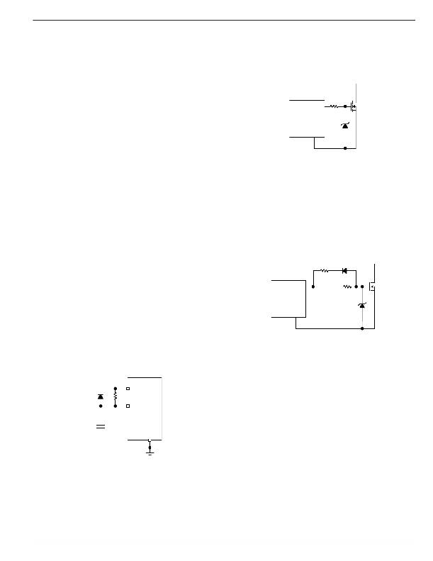
�A� resistor� placed� in� series� with� the� gate� drive� output� attenu-�
�ates� ringing� in� the� etch� connection� between� the� MIC9130�
�and� the� MOSFET.� Figure� 8� shows� a� single� resistor� in� series�
�between� the� driver� output� and� the� gate� of� the� MOSFET.� The�
�zener� value� should� be� greater� than� the� gate� drive� voltage�
�to� prevent� excessive� power� dissipation,� but� less� than� the�
�maximum� gate� to� source� voltage� rating.�
�Gate� Drive�
�Output�
�GND�
�Figure� 8�
�The� circuitry� shown� in� ?� gure� 9� allow� different� rise� and� fall� times.�
�R1� and� the� input� capacitance� of� the� MOSFET� determine� the�
�rise-time� of� the� gate� voltage� and� therefore� the� turn-on� time� of�
�the� MOSFET.� The� diode,� D1� is� reversed� biased,� which� removes�
�R2� from� the� circuit.� At� turn-off,� D1� is� forward� biased� and� the�
�parallel� combination� of� R1� and� R2� controls� the� turn-off� time�
�of� the� MOSFET.� The� turn� on-time� is� slower,� which� reduces�
�switching� noise� and� ringing� during� turn-on.� The� turn-off� time�
�is� faster,� which� minimizes� switching� losses� during� turn-off� and�
�improves� ef� ?� ciency.� If� the� turn-on� time� is� to� be� faster� than�
�the� turn-off� time,� the� diode� should� be� reversed.�
�in� the� MOSFET� is� minimized� under� short� circuit� or� overcur-�
�rent� conditions.�
�If� the� CPWR� pin� is� low� an� overcurrent� or� short� circuit� condi-�
�tions� will� not� trip� the� soft� start� circuit.� The� pulse-by-pulse�
�current� limit,� inherent� in� current� mode� control,� provides� a�
�“brick� wall”� or� constant� current� limit.� With� the� power� supply�
�operating� in� this� mode,� a� smaller� soft� start� capacitor� can� be�
�used� to� increase� the� turn� on� speed� of� the� supply.�
�Gate� Drive�
�Output�
�GND�
�R2�
�D1�
�R1�
�If� the� CPWR� in� is� held� low� during� the� initial� turn� on� at� power�
�up� and� then� raised� high,� the� power� supply� can� maximize�
�the� turn-on� time� at� start� up� and� still� provide� a� high� level� of�
�overcurrent� and� short� circuit� protection.� The� circuit� shown�
�in� Figure� 7� performs� this� function.�
�MIC9130�
�V� REF�
�Figure� 9�
�A� gate� drive� transformer� is� used� where� an� increase� in� drive�
�voltage,� isolation� and/or� voltage� level� shifting� are� required.�
�Gate� drive� transformers� can� have� multiple� windings� and� drive�
�multiple� MOSFETs,� including� MOSFETs� that� require� a� drive�
�signal� 180� degrees� out� of� phase� with� the� ICs� drive� signal.�
�D1�
�R1�
�CPWR�
�Figure� 10� shows� a� gate� drive� transformer� circuit.� The� ca-�
�pacitor,� C1� removes� DC� from� the� drive� circuit� and� prevents�
�C1�
�AGND�
�Figure� 7�
�MOSFET� Gate� Drive� Output�
�The� MIC9130� has� the� capability� to� directly� drive� the� gate� of�
�a� MOSFET.� The� output� driver� consists� of� a� complimentary�
�P-channel� and� N-channel� pair.� The� typical� switching� time�
�of� the� output� is� dependent� on� the� IC� supply� voltage� and� the�
�gate� charge� required� to� turn� the� MOSFET� on� and� off.�
�transformer� saturation.� R1� provides� damping� to� eliminate�
�ringing� in� the� circuit.� R1� is� usually� in� the� 5� to� 20� Ω� range,�
�depending� on� the� amount� of� damping� necessary.� D1� and�
�D2� form� a� clamp� circuit,� which� prevents� the� voltage� from�
�exceeding� the� V� GMAX� level.� If� the� gate� drive� is� well� damped,�
�the� diodes� may� be� removed� R2� is� used� to� allow� the� trans-�
�former� to� reset� properly.�
�November� 2008�
�13�
�M9999-111108�
�相关PDF资料 |
PDF描述 |
|---|---|
| MIC5270-3.0YM5 TR | IC REG LDO -3V .1A SOT23-5 |
| 1945-25J | COIL RF 270UH MOLDED UNSHIELDED |
| VE-J23-CZ | CONVERTER MOD DC/DC 24V 25W |
| 1945-24J | COIL RF 220UH MOLDED UNSHIELDED |
| ADM8839ACPZ | IC CHARGE PUMP REG TFT 20LFCSP |
相关代理商/技术参数 |
参数描述 |
|---|---|
| MIC9130YQS TR | 功能描述:电流型 PWM 控制器 SO-16 High Vin Telecom DC/DC PWM Control IC (Lead Free) RoHS:否 制造商:Texas Instruments 开关频率:27 KHz 上升时间: 下降时间: 工作电源电压:6 V to 15 V 工作电源电流:1.5 mA 输出端数量:1 最大工作温度:+ 105 C 安装风格:SMD/SMT 封装 / 箱体:TSSOP-14 |
| MIC9131 | 制造商:MICREL 制造商全称:Micrel Semiconductor 功能描述:High-Voltage, High-Speed Telecom |
| MIC9131_06 | 制造商:MICREL 制造商全称:Micrel Semiconductor 功能描述:High-Voltage, High-Speed Telecom |
| MIC9131BM | 功能描述:IC CTRLR DC-DC PWM HV HS 16-SOIC RoHS:否 类别:集成电路 (IC) >> PMIC - 稳压器 - 专用型 系列:- 产品培训模块:Lead (SnPb) Finish for COTS Obsolescence Mitigation Program 标准包装:2,000 系列:- 应用:电源,ICERA E400,E450 输入电压:4.1 V ~ 5.5 V 输出数:10 输出电压:可编程 工作温度:-40°C ~ 85°C 安装类型:表面贴装 封装/外壳:42-WFBGA,WLCSP 供应商设备封装:42-WLP 包装:带卷 (TR) |
| MIC9131BM TR | 功能描述:IC CTRLR DC-DC PWM HV HS 16-SOIC RoHS:否 类别:集成电路 (IC) >> PMIC - 稳压器 - 专用型 系列:- 产品培训模块:Lead (SnPb) Finish for COTS Obsolescence Mitigation Program 标准包装:2,000 系列:- 应用:电源,ICERA E400,E450 输入电压:4.1 V ~ 5.5 V 输出数:10 输出电压:可编程 工作温度:-40°C ~ 85°C 安装类型:表面贴装 封装/外壳:42-WFBGA,WLCSP 供应商设备封装:42-WLP 包装:带卷 (TR) |
发布紧急采购,3分钟左右您将得到回复。