- 您现在的位置:买卖IC网 > PDF目录98018 > MJE18002AS (ON SEMICONDUCTOR) 2 A, 450 V, NPN, Si, POWER TRANSISTOR PDF资料下载
参数资料
| 型号: | MJE18002AS |
| 厂商: | ON SEMICONDUCTOR |
| 元件分类: | 功率晶体管 |
| 英文描述: | 2 A, 450 V, NPN, Si, POWER TRANSISTOR |
| 封装: | PLASTIC, TO-220AB, 3 PIN |
| 文件页数: | 1/65页 |
| 文件大小: | 409K |
| 代理商: | MJE18002AS |
当前第1页第2页第3页第4页第5页第6页第7页第8页第9页第10页第11页第12页第13页第14页第15页第16页第17页第18页第19页第20页第21页第22页第23页第24页第25页第26页第27页第28页第29页第30页第31页第32页第33页第34页第35页第36页第37页第38页第39页第40页第41页第42页第43页第44页第45页第46页第47页第48页第49页第50页第51页第52页第53页第54页第55页第56页第57页第58页第59页第60页第61页第62页第63页第64页第65页
3–704
Motorola Bipolar Power Transistor Device Data
Designer's Data Sheet
SWITCHMODE
NPN Bipolar Power Transistor
For Switching Power Supply Applications
The MJE/MJF18002 have an applications specific state–of–the–art die designed
for use in 220 V line operated Switchmode Power supplies and electronic light
ballasts. These high voltage/high speed transistors offer the following:
Improved Efficiency Due to Low Base Drive Requirements:
— High and Flat DC Current Gain hFE
— Fast Switching
— No Coil Required in Base Circuit for Turn–Off (No Current Tail)
Tight Parametric Distributions are Consistent Lot–to–Lot
Two Package Choices: Standard TO–220 or Isolated TO–220
MJF18002, Case 221D, is UL Recognized at 3500 VRMS: File #E69369
MAXIMUM RATINGS
Rating
Symbol
MJE18002
MJF18002
Unit
Collector–Emitter Sustaining Voltage
VCEO
450
Vdc
Collector–Emitter Breakdown Voltage
VCES
1000
Vdc
Emitter–Base Voltage
VEBO
9.0
Vdc
Collector Current — Continuous
— Peak(1)
IC
ICM
2.0
5.0
Adc
Base Current — Continuous
— Peak(1)
IB
IBM
1.0
2.0
Adc
RMS Isolated Voltage(2)
Test No. 1 Per Fig. 1
(for 1 sec, R.H. < 30%,
Test No. 2 Per Fig. 2
TC = 25°C)
Test No. 3 Per Fig. 3
VISOL
—
4500
3500
1500
V
Total Device Dissipation
(TC = 25°C)
Derate above 25
°C
PD
50
0.4
25
0.2
Watts
W/
°C
Operating and Storage Temperature
TJ, Tstg
– 65 to 150
°C
THERMAL CHARACTERISTICS
Rating
Symbol
MJE18002
MJF18002
Unit
Thermal Resistance — Junction to Case
— Junction to Ambient
R
θJC
R
θJA
2.5
62.5
5.0
62.5
°C/W
Maximum Lead Temperature for Soldering
Purposes:
1/8
″ from Case for 5 Seconds
TL
260
°C
ELECTRICAL CHARACTERISTICS (TC = 25°C unless otherwise noted)
Characteristic
Symbol
Min
Typ
Max
Unit
OFF CHARACTERISTICS
Collector–Emitter Sustaining Voltage (IC = 100 mA, L = 25 mH)
VCEO(sus)
450
—
Vdc
Collector Cutoff Current (VCE = Rated VCEO, IB = 0)
ICEO
—
100
Adc
Collector Cutoff Current (VCE = Rated VCES, VEB = 0)
TC = 125°C
Collector Cutoff Current (VCE = 800 V, VEB = 0)
TC = 125°C
ICES
—
100
500
100
Adc
Emitter Cutoff Current (VEB = 9.0 Vdc, IC = 0)
IEBO
—
100
Adc
(1) Pulse Test: Pulse Width = 5.0 ms, Duty Cycle
≤ 10%.
(continued)
(2) Proper strike and creepage distance must be provided.
Designer’s Data for “Worst Case” Conditions — The Designer’s Data Sheet permits the design of most circuits entirely from the information presented. SOA Limit
curves — representing boundaries on device characteristics — are given to facilitate “worst case” design.
Preferred devices are Motorola recommended choices for future use and best overall value.
MOTOROLA
SEMICONDUCTOR TECHNICAL DATA
MJE18002
MJF18002
POWER TRANSISTOR
2.0 AMPERES
1000 VOLTS
25 and 50 WATTS
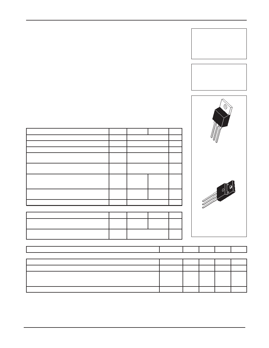
CASE 221A–06
TO–220AB
MJE18002
CASE 221D–02
ISOLATED TO–220 TYPE
UL RECOGNIZED
MJF18002
*
*Motorola Preferred Device
REV 1
相关PDF资料 |
PDF描述 |
|---|---|
| MJE18002AN | 2 A, 450 V, NPN, Si, POWER TRANSISTOR |
| MJE18002BA | 2 A, 450 V, NPN, Si, POWER TRANSISTOR |
| MJE18002BG | 2 A, 450 V, NPN, Si, POWER TRANSISTOR |
| MJE18002AF | 2 A, 450 V, NPN, Si, POWER TRANSISTOR |
| MJE18002AK | 2 A, 450 V, NPN, Si, POWER TRANSISTOR |
相关代理商/技术参数 |
参数描述 |
|---|---|
| MJE18002D2 | 制造商:Rochester Electronics LLC 功能描述:- Bulk |
| MJE18002G | 功能描述:两极晶体管 - BJT 2A 450V 40W NPN RoHS:否 制造商:STMicroelectronics 配置: 晶体管极性:PNP 集电极—基极电压 VCBO: 集电极—发射极最大电压 VCEO:- 40 V 发射极 - 基极电压 VEBO:- 6 V 集电极—射极饱和电压: 最大直流电集电极电流: 增益带宽产品fT: 直流集电极/Base Gain hfe Min:100 A 最大工作温度: 安装风格:SMD/SMT 封装 / 箱体:PowerFLAT 2 x 2 |
| MJE18004 | 功能描述:两极晶体管 - BJT 5A 1000V 75W NPN RoHS:否 制造商:STMicroelectronics 配置: 晶体管极性:PNP 集电极—基极电压 VCBO: 集电极—发射极最大电压 VCEO:- 40 V 发射极 - 基极电压 VEBO:- 6 V 集电极—射极饱和电压: 最大直流电集电极电流: 增益带宽产品fT: 直流集电极/Base Gain hfe Min:100 A 最大工作温度: 安装风格:SMD/SMT 封装 / 箱体:PowerFLAT 2 x 2 |
| MJE18004D2 | 功能描述:两极晶体管 - BJT 5A 1000V 75W NPN RoHS:否 制造商:STMicroelectronics 配置: 晶体管极性:PNP 集电极—基极电压 VCBO: 集电极—发射极最大电压 VCEO:- 40 V 发射极 - 基极电压 VEBO:- 6 V 集电极—射极饱和电压: 最大直流电集电极电流: 增益带宽产品fT: 直流集电极/Base Gain hfe Min:100 A 最大工作温度: 安装风格:SMD/SMT 封装 / 箱体:PowerFLAT 2 x 2 |
| MJE18004D2G | 功能描述:两极晶体管 - BJT 5A 1000V 75W NPN RoHS:否 制造商:STMicroelectronics 配置: 晶体管极性:PNP 集电极—基极电压 VCBO: 集电极—发射极最大电压 VCEO:- 40 V 发射极 - 基极电压 VEBO:- 6 V 集电极—射极饱和电压: 最大直流电集电极电流: 增益带宽产品fT: 直流集电极/Base Gain hfe Min:100 A 最大工作温度: 安装风格:SMD/SMT 封装 / 箱体:PowerFLAT 2 x 2 |
发布紧急采购,3分钟左右您将得到回复。